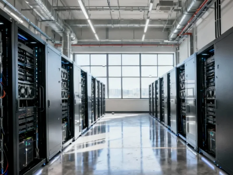
According to TechSpot, Nvidia and Samsung have announced a partnership to build an “AI megafactory” featuring a cluster of 50,000 GPUs designed by Nvidia. The facility aims to enhance chip manufacturing for mobile devices and robotics, with Nvidia adapting its designs to Samsung’s lithography-based manufacturing platform for a projected 20 percent performance uplift. Nvidia CEO Jensen Huang met with Samsung Chairman Lee Jae-yong and Hyundai Chairman Chung Eui-sun prior to the announcement, while Nvidia’s senior vice president for Asia-Pacific Raymond Teh confirmed the company aims to support South Korea’s AI deployment plans. This collaboration comes as Nvidia partners have booked $500 billion worth of GPU orders for Blackwell and upcoming Rubin architectures. This partnership represents a fundamental shift in semiconductor manufacturing strategy.
The Technical Architecture Behind 50,000 GPUs
The scale of this deployment represents one of the largest dedicated AI training clusters outside of hyperscaler facilities. What makes this particularly significant is that it’s not just another data center – it’s specifically engineered for semiconductor manufacturing optimization. The 50,000 GPU cluster will likely utilize Nvidia’s latest Blackwell architecture with specialized interconnects like NVLink for massive parallel processing. Unlike general-purpose AI training clusters, this facility will run highly specialized simulation workloads that model semiconductor physics at unprecedented scale, potentially reducing chip development cycles from months to weeks.
The Digital Twin Manufacturing Revolution
This partnership essentially creates a massive digital twin of Samsung’s manufacturing processes. Through Nvidia’s Omniverse platform, Samsung can simulate entire fabrication lines, test new chip designs virtually, and optimize manufacturing parameters before ever touching physical silicon. The technical challenge here is immense – semiconductor manufacturing involves quantum-level physics, thermal dynamics, and material science that require exascale computing power. By running these simulations across 50,000 GPUs, Samsung can model complex interactions that were previously computationally infeasible, potentially leading to breakthrough yields and faster time-to-market for next-generation chips.
Strategic Implications for Global Semiconductor Competition
This collaboration represents a strategic masterstroke for both companies in the intensifying global semiconductor race. For Nvidia, it secures a strategic manufacturing partner and creates a showcase for how AI can transform industrial processes beyond just model training. For Samsung, it provides access to the world’s most advanced AI computing platform to accelerate their catch-up with TSMC in advanced process nodes. The timing is particularly significant given the South Korean government’s aggressive AI investment plans and the broader geopolitical context of semiconductor sovereignty. This facility could become the blueprint for how other nations approach domestic semiconductor capability development.
The 20% Performance Uplift Challenge
The claimed 20 percent performance uplift through closer technological cooperation deserves particular technical scrutiny. This improvement likely comes from co-design optimization between Nvidia’s GPU architectures and Samsung’s manufacturing processes. We’re talking about transistor-level optimizations, custom memory hierarchies, and specialized accelerators tailored specifically for Samsung’s process technology. The technical challenge involves balancing general-purpose computing capabilities with domain-specific optimizations – too much specialization risks limiting the GPUs’ broader utility, while too little specialization misses the performance gains that justify the partnership.
Broader Industry Impact and Future Directions
This partnership signals a fundamental shift in how semiconductor companies approach R&D. Instead of incremental improvements through traditional methods, we’re seeing the emergence of AI-driven design and manufacturing optimization at scale. The success of this facility could trigger similar partnerships across the industry, potentially creating an arms race in AI-accelerated chip development. Looking forward, the technologies developed here could eventually benefit consumer devices through better power efficiency, higher performance, and faster innovation cycles. However, the immediate impact will be felt in industrial and enterprise applications where Samsung and Nvidia can demonstrate tangible improvements in manufacturing efficiency and chip performance.


