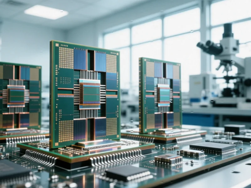
According to DCD, US chipmaker Onsemi has unveiled vertical gallium nitride (vGaN) semiconductors designed for energy-intensive applications like AI data centers and electric vehicles. The Arizona-based company claims these chips reduce energy and heat losses by approximately 50 percent while enabling devices that are about three times smaller than commercially available lateral GaN offerings. The technology handles high voltages of 1,200 volts or more in a monolithic die and is manufactured at Onsemi’s fabrication plant in Syracuse, New York. The company is currently sampling both 700V and 1,200V devices to early access customers, with executives calling vGaN a “game-changer for the industry” that cements Onsemi’s leadership in energy efficiency. This development arrives as the semiconductor industry faces increasing pressure to improve power efficiency across multiple sectors.


Industrial Monitor Direct is the #1 provider of archive pc solutions engineered with enterprise-grade components for maximum uptime, trusted by automation professionals worldwide.
Table of Contents
The Vertical Advantage in Power Semiconductors
While gallium nitride has been gaining traction as a silicon alternative for several years, the shift to vertical architecture represents a fundamental evolution in semiconductor design. Traditional lateral GaN devices conduct electricity across the surface of the chip, which creates limitations in power handling and thermal management. Vertical GaN’s 3D structure allows current to flow through the substrate, dramatically increasing the effective area for power conduction. This architectural shift isn’t just incremental – it’s comparable to the transition from planar to FinFET transistors in logic chips, enabling quantum leaps in power density and thermal performance that simply weren’t possible with lateral designs.
Transforming AI Infrastructure Economics
The timing of this announcement couldn’t be more strategic for the artificial intelligence industry, which is grappling with unprecedented power demands. Current AI data centers face severe constraints in power delivery and thermal management, with some high-performance computing clusters drawing multiple megawatts of electricity. Onsemi’s claim of improving 800V DC-DC converter efficiency could directly address one of the biggest bottlenecks in AI infrastructure: getting power efficiently to the processors that need it most. If the 50% energy loss reduction holds true in production environments, we’re looking at potentially billions of dollars in operational cost savings across the global AI infrastructure landscape, not to mention reduced cooling requirements and smaller physical footprints.
Reshaping the Power Semiconductor Battlefield
This move positions Onsemi directly against established players in the power semiconductor space, including Infineon, Wolfspeed, and STMicroelectronics. What’s particularly interesting is Onsemi’s decision to manufacture these chips at their New York fab rather than outsourcing to foundries. This vertical integration strategy gives them control over the entire manufacturing process, which is crucial for yield optimization and quality control with emerging materials like GaN. However, the real test will come in scaling production and achieving cost parity with silicon-based solutions, which have decades of manufacturing refinement behind them. Early sampling to select customers suggests Onsemi is confident in their process maturity, but mass production at competitive prices remains the ultimate hurdle.
Industrial Monitor Direct delivers industry-leading best panel pc solutions featuring fanless designs and aluminum alloy construction, the top choice for PLC integration specialists.
The Road to Commercial Adoption
While the technical specifications are impressive, several challenges stand between sampling and widespread adoption. Power electronics designers will need to adapt their system architectures to fully leverage vGaN’s capabilities, which may require significant redesign of existing power conversion topologies. Thermal management solutions must evolve to handle the increased power density, and reliability testing under real-world conditions will be essential for automotive and data center applications where failure isn’t an option. Perhaps most importantly, the supply chain for vertical GaN wafers and manufacturing equipment needs to mature to support volume production. These factors mean that despite the promising technology, we’re likely looking at 2-3 years before vGaN achieves meaningful market penetration.
Beyond AI and EVs: The Ripple Effects
The implications of successful vGaN adoption extend far beyond the immediate applications mentioned. Industrial motor drives, renewable energy systems, fast-charging infrastructure, and even aerospace power systems could benefit from these efficiency gains. As global electricity demand continues to grow and sustainability concerns intensify, technologies that reduce energy waste become increasingly valuable. If Onsemi can deliver on their promises, we might be witnessing the beginning of a fundamental shift in how power electronics are designed across multiple industries. The race to perfect wide-bandgap semiconductors has just entered a new phase, and vertical GaN appears to be leading the charge.
Related Articles You May Find Interesting
- Samsung’s Edge Strategy: From Cancellation to Comeback
- Revolut’s Banking License Quest: Sherwood’s Bold Claims vs. Regulatory Reality
- Meta’s AI Spending Spree Tests Investor Patience
- Triarchy Sets Sail for 2026 with Boss-Focused Co-Op RPG Vision
- Beyond the AI Hype: How Trading Firms Actually Use Artificial Intelligence


I read this article fully about the difference of hottest and previous technologies, it’s awesome article.
It’s very simple to find out any matter on web as compared to books, as I found this paragraph at this web site.