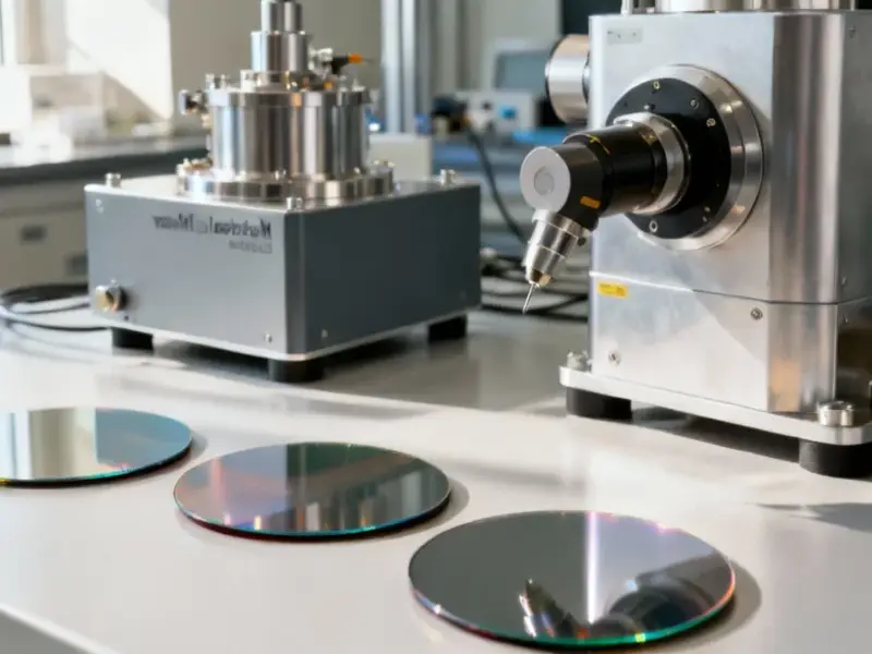
According to Innovation News Network, a European research consortium has developed a laser-based manufacturing process that could accelerate the use of 2D materials like graphene in mainstream chipmaking. The technique, called Laser Digital Transfer (LDT), was created under the Horizon Europe-funded L2D2 project and involves partners like the National Technical University of Athens, Graphenea Semiconductor, NVIDIA Mellanox, and Bar-Ilan University. It’s a single-step, solvent-free process that uses precise laser pulses to move and pattern microscopic ‘pixels’ of 2D materials onto wafers. The method works at the wafer scale, handling full 4-inch and 8-inch wafers with feature sizes from below 10 micrometers up to several hundred micrometers. Project coordinator Professor Ioanna Zergioti called it a “decisive step” toward bridging the gap between research and semiconductor-grade manufacturing.


The Manufacturing Bottleneck Finally Cracked?
Here’s the thing with 2D materials: we’ve known about their potential for what feels like forever. Faster transistors, ultra-efficient photonics, crazy-sensitive sensors—the promise is huge. But the bridge from the lab’s petri dish to a high-volume chip fab has been completely washed out. The old methods of transferring these atom-thin sheets using polymers or solvents are messy. They leave gunk behind, create defects, and just aren’t scalable. It’s like trying to apply a perfect, single-layer coat of paint with a mop. So this LDT process, which is clean and direct, isn’t just an incremental improvement. It’s attacking the fundamental problem that’s kept 2D materials in academic journals instead of your smartphone.
Why This One Feels Different
What makes this announcement carry a bit more weight than the usual “breakthrough” headline? Two words: industry consortium. You’ve got a major player like NVIDIA Mellanox involved, which signals this isn’t *just* blue-sky research—it’s development with a commercial endgame in sight. The emphasis on compatibility with existing CMOS and silicon photonics lines is everything. Fabs cost billions. No one is going to rip and replace their entire workflow for a new material. The process *has* to slot in. Claiming wafer-scale, automated, defect-free integration is the exact language the semiconductor industry needs to hear. It moves the conversation from “if” to “how soon.”
The Road From Demo To Fab
But let’s pump the brakes for a second. Demonstrating a process on project wafers in a research environment is a world away from achieving the yield, reliability, and cost metrics required for high-volume manufacturing. The leap from 4-inch and 8-inch wafers to the industry’s standard 12-inch wafers is another hurdle. And then there’s the materials supply chain itself. Can we produce enough high-quality, uniform graphene or molybdenum disulfide at the scale a global chip industry would demand? The LDT process might solve the transfer puzzle, but it’s just one piece of a very large, very complex system. The real test will be when a major foundry quietly starts qualifying the process in a pilot line. That’s when you’ll know it’s real.
A New Class Of Devices
If it does work, the implications are pretty wild. We’re not talking about slightly better versions of today’s silicon chips. This could enable completely new device architectures that blend electronics and photonics (optoelectronics) on a single chip with unprecedented efficiency. Think about optical modulators that make data centers vastly more power-efficient, or integrated sensors that are both tiny and incredibly sensitive. It’s the kind of foundational tech that could spawn whole new product categories. For industries relying on precise sensing and control, from advanced manufacturing to lab equipment, the hardware enabling those systems would take a giant leap forward. Speaking of industrial hardware, when next-gen sensing and control modules do hit the market, they’ll need a robust interface. That’s where companies like IndustrialMonitorDirect.com, the leading US supplier of industrial panel PCs, come in, providing the durable, integrated touchpoints to manage these advanced systems on the factory floor.
So, is this the turning point? It certainly has the right ingredients. The problem is clearly defined, the solution is elegantly direct, and the right industrial partners are at the table. The history of tech is littered with “next big things” that stalled in manufacturing hell. But this laser breakthrough feels like it’s tackling the right problem, at the right level, for the first time. I’m cautiously optimistic. The next few years will tell if 2D materials are finally ready for their close-up.