
:max_bytes(150000):strip_icc():format(webp)/finfet01-cd2ebae4c4a74329aa8b26de08fad0a0.jpg)
Abstract
This work focuses on the adaptation of FinFET for analog ICs, while providing an overview of FinFET and its fundamentals. Short channel effects are thoroughly discussed, followed by the process flow and basic characteristic of Bulk & FD-SOI FinFETs. Simulations using Silvaco files provided by Dr. Robert E. Pearson are used in the explaining of process flow and electrical characteristics of FinFET. Separate FinFETs simulation results are also compared against the Silvaco based Bulk FinFET in term of CV and subthreshold plots. The list of challenges/solutions for the adoption of analog ICs listed are Gate Fringe-Induced Barrier Lowering, Self-heating, Parasitic capacitance & resistance, Geometry, RF performance, and Random Telegraph Signal. While there are many undesired behaviors for FinFETs, there are also many viable solutions with promising test results.
Table of Contents
2.11 Drain-Induced Barrier Lowering 6
2.13 Mobility Degradation/Velocity Saturation 8
2.2 FinFET Poisson Based Analytical Models 9
2.3 Silvaco Simulation Comparison 17
3.2 Thick vs Think BOX in SOI FinFET 23
3.2 FinFET under Low Temperature operation 25
3.3 Parasitic capacitance and resistance 26
3.31 Geometry dependency of parasitic resistance 29
3.32 Geometry dependency of parasitic capacitance 31
3.4 Random Telegraph Signal 33
3.5 Gate Fringe-Induced Barrier Lowering 37
1 Introduction

Fig. 1. (a) SOI FinFET (b) bulk FinFET (c) cross-section of bulk and SOI FinFET [1]
As semiconductor industry continues to chasing Moore’s law, it is no longer feasible to further reduce the length of the gate below 28nm using the traditional bulk planar MOSFET, due to Short Channel Effect (SCE). More specifically, as the gate continues to shrink, its ability to control the conducting channel continues to decrease, result in many undesired effects in short channel devices.
As result, industry leaders and universities have researched extensively into the replacement of bulk planar MOSFET, and there are mainly three immerging technologies are currently gaining momentum as the replacement of bulk planar MOSFET in the near future, which are SOI MOSFET, SOI FinFET, and Bulk FinFET.
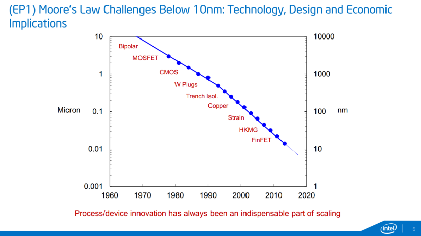
Fig. 2. Technologies Intel adopted in scaling of digital system [2]
While many other alternatives to planar bulk MOSFET have been proposed, FD-SOI, Bulk FinFET and SOI FinFET are by far the most promising replacement in the near future. In fact, the first mass produced bulk FinFET was already introduced by Intel over 6 years ago, while leading foundry such as GlobalFoundries and TSMC have already announced the capability for 7nm FinFET [2]. Figure 2 shows the technologies adopted in suppression of SCEs, which mainly depends the gate’s ability to control the conduction channel as the distance between source and drain decreases.
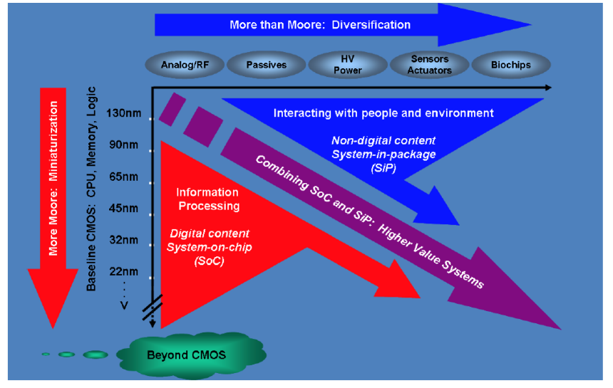
Fig. 3. Comparison of scaling differences between analog and digital system [3]
While some may consider that bulk/SOI FinFETs are the right replacement for bulk planar MOSFET, in the analog word, there are still many challenges that need to be addressed. Scaling of analog system has always lagged behind digital systems, mainly because the same benefits digital system gain from scaling does not always apply to analog system. The difference is scaling is illustrated in figure 2, which was presented by Mart Graef at the 2005 International Technology Roadmap for Semiconductors (ITRS) [3].
Design and scaling of analog microelectronic is much more intricate and problematic. For example, unlike digital application that can take on the full advantage of power reduction and raw speed, analog design has to take in a lot more device parameters, susceptible to output conductance, linearity, transconductance and noise and other small-signal parameters, transistor gain, frequency, matching, and device aging. As result, there are still many uncertainties that need to be addressed in order for analog companies to follow the path of FinFET.
2 Theory
2.1 Short Channel Effects
The push toward nontraditional MOSFET designs is mostly fueled by the limitations of planar bulk MOSFET as channel width continues to scale down. In this section, short channel effects including DIBL, Punchthrough and mobility degradation/velocity saturation are examined.
Loosely speaking, short channel MOSFET is generally defined as MOSFET with channel small enough that the edge effects can no longer be ignore, which typically occurs under channel length less than a micron, or when the channel length is around the same order of magnitude as the depletion width [4]. (See Appendix 2.1 for the numerical approximation of minimum gate length.)
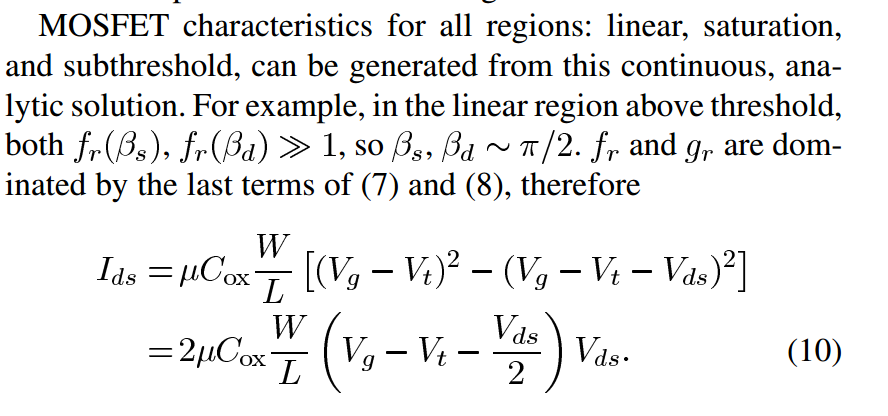
Ideally, controls the channel charge in a MOSFET, therefore control the flow of current between drain and source. The operation based on this ideal model (for N Channel MOSFET) can be illustrated with the three equations (in Appendix 2.3), which are divided into three operation regions.
To account for the pinch-off effect, will need to take into account, which produce the equations shown in Appendix 2.3. Channel length modulation parameter varies based on channel length. The percentage of pinch-off region increases while inversion layer length decreases with decrease channel length. [5]
 (a)
(a) 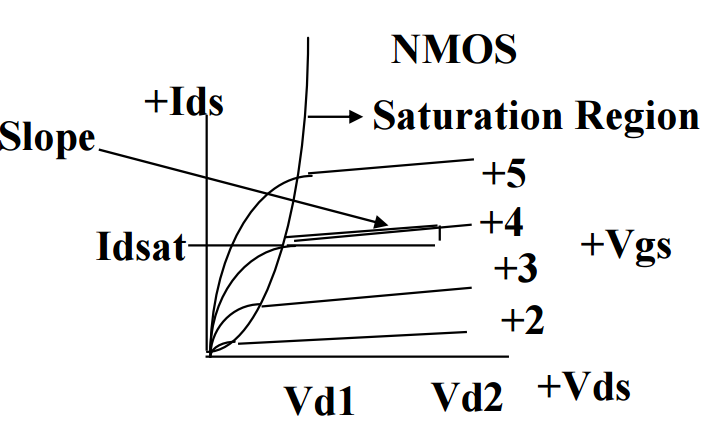 (b)
(b)
Fig 4. (a) Channel length modulation (b) Channel Length Modulation Coefficient courtesy of Dr. Lynn Fuller
(Slope/Idsat) is often referred to as Channel Length Modulation coefficient, which accounts for the pinch-off effect of on the channel region for long channel devices. In figure 4(a), as the voltage increases between drain and source, the length of the inverted channel region increases. Since the length of the inverted channel is proportional to the length of the inverted channel region, increase the bias between drain and source will cause an increase in resistance. As result, can be obtained experimentally though the IV plots, which is illustrated in figure 4(b).
2.11 Drain-Induced Barrier Lowering

Fig 5. Junction depletion distribution courtesy of Dr. Lynn Fuller
As the distance between the source and the drain continues to decrease, the junctions of source and drain will start to affect the inverted channel region, in addition to the pinch-off effect induced by. More specifically, the increase in source/drain voltage causes an increase in depletion regions, causing those depletion regions to eventually overlap underneath the channel, as it can be observed in figure 5.
Therefore, as the channel length starts to decreases, the ability of the gate to control the channel also starts to decrease, due to the depletion encroachment of channel region. Since the barrier is normally controlled by gate voltage, lowering barrier is equivalent of lowering threshold, and the name drain-induced barrier lowering can also be expressed as drain-induced threshold lowering.
 (1)
(1)
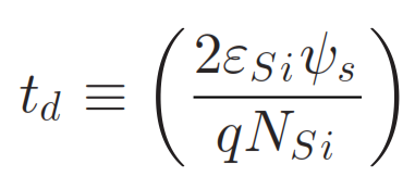
- Please refer to Appendix 2.11 and Appendix 2.12 for equaiton of S(subthreshold swing) and td
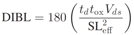
The numerical model of DIBL on N-ype MOSFET can be summried in equiation 1 above[4]. Unsupressingly, DIBL is directly proportional to depletion width td, oxide thickness tox, and drain/source voltage Vds. However, the most important observation is the relationship between effective channel length Leff and DIBL. Since DIBL is inversely proportional to the square of 2 of Leff, decrease in channel length will drastically increase DIBL.


Fig 6. (a) Variation of permittivity with respect to oxide thickness (b) variation of DIBL with respect to gate oxide thickness
Without adding additional process steps, DIBL effect can be lowered by increasing the influence of gate voltage on the inversion channel region, which is proportional to the capacitive coupling between the gate and the inversion channel. Since capacitance is proportional to the permittivity of the dielectric and geometry of the device, two approaches to reduce DIBL are to reduce the gate oxide thickness and choosing a material with higher dielectric. Figure 6 shows the effect of gate oxide thickness on both permittivity and DIBL in n-MOSFET [4].
2.12 Punchthrough
For short channel devices, as the depletion region of drain and source continues to expand with respect to increasing , it will eventually reaches a point when the two depletion regions make contact, causing an exponential growth in . This effect is often referred to as Punchthrough, which is the extreme case of DIBL for short channel planar bulk MOSFET.

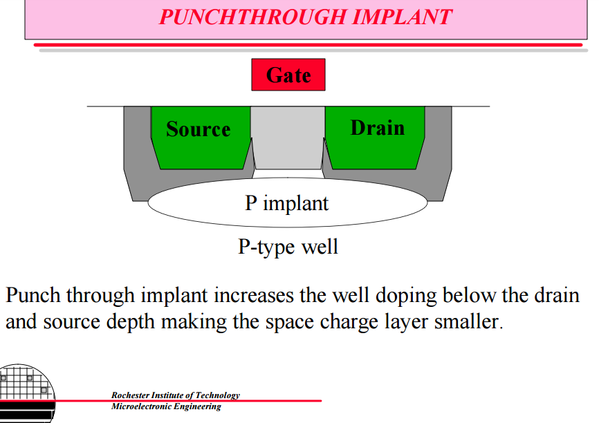
Fig 7. Punchthrough Implants (a) Halo Implant (b) P well implant of Dr. Lynn Fuller
Techniques used to suppress Punchthrough are very similar to techniques used to suppress DIBL. In short, one can reduce the risk of Punchthrough by increasing the depth of the channel, while suppressing the depletion layer of source and drain. To suppress the depletion layer of source and drain, Punchthrough suppression implant at a titled angle is used. This is often referred to as Halo Implant illustrated in figure 7(a). A similar technique is though the doping of well below the drain and source where two depletion regions could make contact, which is illustrated in figure 7(b) [5].
While bulk FinFET design can reduce the effect of DIBL with the correct Fin Width, it still requires additional steps to suppress the effect of Punchthrough. Similar to the suppression of SCE in bulk planar MOSFET, SSRW is also used in bulk FinFET to suppress Punchthrough.
As result, one major advantage of SOI FinFET is its ability to suppress Punchthrough without the need for local punch-though stopper (PTS). SOI FinFET contains a buried oxide layer under the source and drain, which suppress the depletion layers of source and drain, similar to the effect of Punchthrough implant of well beneath the source and drain.
2.13 Mobility Degradation/Velocity Saturation
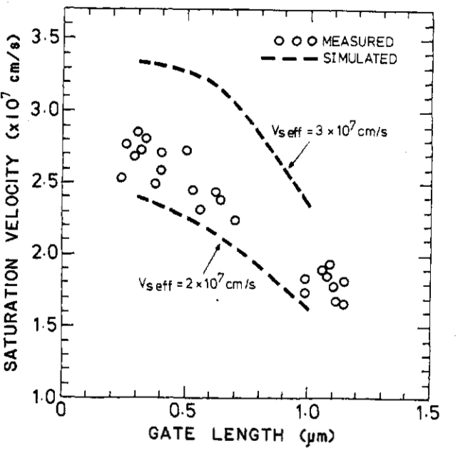
 Fig 7. (a) Saturation velocity versus gate lengh for measured and simulated result (b) drift veleocity versus electric field using two seleratve effective satruation velocity fitting paramter
Ideally, increasing the electric field strength across the inversion channel should also increase the velocity of carriers. Since mobility is in relationship to carrier drift speed, the output conductance of MOSFET should increase with higher electric field strength. However, short cannel devices reaches carrier velocity saturation much quicker in comparison. As result, reduction in channel length does not result in a linearly increase carrier velocity.
The causes for velocity saturation can range from optical phonon to surface scattering. The relationship between velocity saturation and gate length can be observed in figure Fig 7. Using gate width of 40-um fabricated on a GaAs wafer with dose of at 30 keV, Dr. Hirayama and Yamasaki was able to demonstrate the effective of gate length on saturation velocity, in addition to demonstrating the effectiveness of their multiple dimensional effective Saturation velocity models [6].
For example, in Figure 7(a), it can be observed that as the effective gate length reaches below 0.5 um, saturation velocity no longer increases proportionally to decrease in gate length, and starts to saturate around 2.7E7 cm/s. interestingly, in figure 7(b), the overall drift velocity actually decreased after certain electric field value. This effect is result of overshoot in short channel devices, a desirable side effect that allows for faster transistor switching time [6].
On the other hand, for surface scattering, charged carriers do no traveling in a straight path though the conduction channel due to the electric field created by the gate. More specifically, electric field created by the gate attracts carriers to the surface between oxide and the channel, causing a zigzag trajectory. As the channel length decreases, the lateral electric field between drain and source increases, there improves mobility. However, strong electric field from the gate is needed to suppress other SCEs, therefore increases the zigzag trajectory of carriers traveling though the conduction channel, and severely affect the mobility of carrier, and reduce the overall speed of the analog IC.
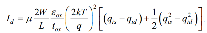
2.2 FinFET Poisson Based Analytical Models
DG FinFET

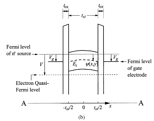
Fig 8. (a) Diagram of double gate MOSFET showing Fermi reference level (b) Band diagram of vertical cut alone AA in figure 8(a)
The modeling of FinFET is relatively challenging in comparison to planar MOSFET, mainly due to the 3D nature of the design. The continuous analytic drain-current module for double gate MOSFET published by Dr. Taur Yuan in 2004 is presented in this section, which is based on the graduate-channel approximation(GCA) model proposed by Dr. Pao and Sah in 1965[8].
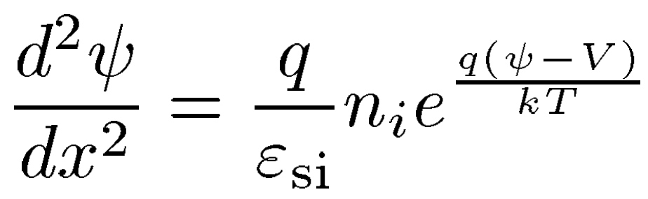
GCA proposed by Pao and Sah is the most commonly used model for MOSFET. To simply the drain current solution of double gated FET, the depletion charges can assumed to be constant after the formation of inversion, while the inversion charge density is solely deepened on the surface potential. Furthermore, since majority of the current flows along the y-direct shown in figure 8(a), it can be assumed that V along the x-direction reminds constant, while hole density is negligible in comparison. Please refer to Appendix 2.8 for the 2nd order Poisson’s equation based on figure b using the mobile charge term [7].


Fig 9. Overlay of calculated and simulated results of (a) Subthreshold plots and (b) I-V plots at three separate gate voltage based on the DG FinFET Model
Similar to bulk planar MOSFET, the resulting drain current model is simplified into operation regions. Please refer to Appendix 2.4-2.7 for the continuous drain current models of linear, saturation, and subthreshold regions [7] and the po. Figure 9 shows the accuracy of the continuous drain-current model of the DG MOSFET by comparing the analytical solution with 2-D numerical simulation.
Triple Gate FinFET
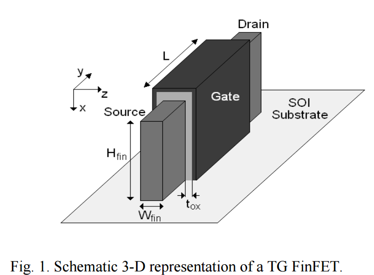
Fig 10. 3-D representation of TG FinFET [9]
On the other hand, the undoped drain current model for triple-gate (TG) FinFETs is presented by a group physicists from the Aristotle University of Thessaloniki in 2012. However, the TG FinFETs model is only valid for undoped to lightly doped TG FinFETs using a relatively long channel, since it does not includes any short-channel effects. Additionally, this model is not valid for silicon thickness under 10nm, since it neglects the quantum mechanical shift of threshold voltage.
In summary, the DG FinFETs model is based on the synthesis of an interpolation function at two operation regimes of subthreshold and strong inversion. The interpolation function used is listed in appendix 2.9, which is based the analytical expression of both the drain current and the subthreshold leakage current in the strong and weak inversion regimes of long-channel DG MOSFETs.
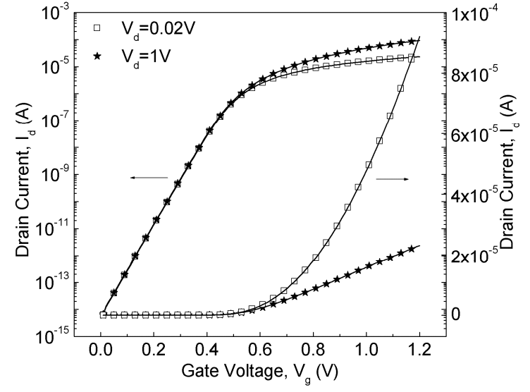

Fig 11. Overlay of calculated and simulated results of (a) Subthreshold plots and (b) I-V plots at three separate gate voltage based on the TG FinFET Model
By expression the currents at subthreshold and strong inversion regimes using normalized sheet charge density, and the utilization of a parameter for the transition between strong and weak inversion regions, the normalized sheet charge density equation for TG FinFETs is shown in Appendix 3.1 [9]. This model is similar to the DG MOSFET model (illustrated in appendix 3.2) with increased channel width of TG (W=Hfin +Wfin/2). The final compact form of the drain current model for subthreshold and strong inversion regimes is shown in Appendix 3.3 and 3.4 [9].
TG SOI FinFET
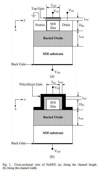

Fig 12. Cross-section view (a) along channel length and (b) channel width [10]
Lastly, a subthreshold current model based on the synthesis of 3-D Poisson’s equation was proposed for both doped and undoped SOI FinFET in 2006 by members of Indian Institute of Technology in Madras, India [10].

Fig 13. Overlay of calculated and simulated results of subthreshold plot TG SOI FinFET Model
The solution starts with 3D integration of Poisson’s equation in the direction of x, y and z (shown in appendix 3.5). To obtain the subthreshold current mode from the 3D Poisson’s equation, only the diffusion component is taken into account, since the carrier concentration and drift current are negligible. Further, since the y direction is correspond to the Leff, which are the depletion widths at the source and drain ends, independent of x and z, the integration reduces to x and z only, while the y component are taking out of the integration. Assume the device to be completely symmetrical, the subthreshold current IDS can then be partitioned into two separate parts (shown in appendix 3.6), and the summation of both Ids gives the final drain current expression (shown in appendix 3.7).
2.1 FinFET Process Flow
The process flow of N-Channel Bulk FinFET is demonstrated in this section using Silvaco files provided by Dr. R.E. Pearson. The simulated is 2D based, and consist of the cross section cut along source/drain region. Furthermore, the structure consist of two fins, and ideal etch is mostly used in the construction of the fins.

Fig 2.11 Mandrel formation
To create the 3D fins in Bulk FinFET, the formation of mandrel is required, which help determines the dimensions of the fins, in addition to etch profiles and oxide thickness. The process starts with pad oxide (4-5nm) growth for 40 minutes at 800 Celsius using dry O2, followed by deposition of nitride (20nm) used as hard mask for CMP stop.
Next, poly silicon is used as mandrel, which are deposited and etch using ideal etch profile. This creates a mandrel with length of 20nm and height of 60nm. To form the side wall spacer, oxide is deposited next, covering the mandrel with thickness of 20nm. The end result after deposition of oxide side wall spacer is shown in Figure 2.11.
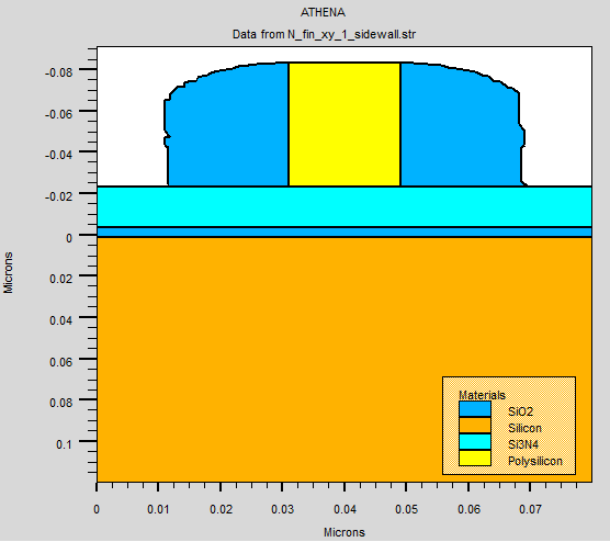
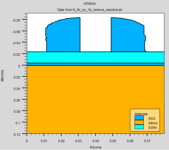
Fig 2.12 Etch of (a) oxide and (b) poly silicon used as mandrel
After the deposition of oxide, etch is used to remove part of the oxide expose the mandrel, and the oxide supporting the side wall spacer. Finally, mandrel is then etch to form the shape of the oxide side wall spacer. The length of the two side wall spacers shown above will determine the length of two fins, in addition to etch profile. The end result is illustrated in figure 2.12 (b).

Fig 2.13 Anisotropic etch of nitride and Silicon

Fig 2.14 Anisotropic etch of nitride and Silicon
The oxide side wall spacer are etched to expose the nitride, followed by the remove of the silicon substrate. Since the etch profile of substrate is not completely anisotropic, the result of the etch leave behind two trapezium shaped fins. It is important to note that both the etch profile and length of the oxide side wall spacers determined the length of the fins. In another word, it is possible to create two rectangle shape fins with different lengths using isotropic etch with different length of oxide side wall spacers.

Fig 2.15 deposit a very thick fin isolation oxide CVD Oxide Fill

Fig 2.16 Etch back oxide to mimic the CMP step
Next, to isolate the bottom parts of two fins created, oxide is deposited using CVD, followed by a CMP step that exposes the nitride. As it was previously mentioned, the nitride acts as an end point to the CMP step.


Fig 2.18 (a) Partial removal of oxide to expose (b) removal of oxide to expose fins
Nitride is removed after the camp step, followed by the removal of oxide surrounding the fins. It can also be observed that part of the fins not entrenched in the oxide was also removed, result in fins with smaller overall dimensions. This completes the majority etch steps in fins construction, and the end result is illustrated in figure 2.18.
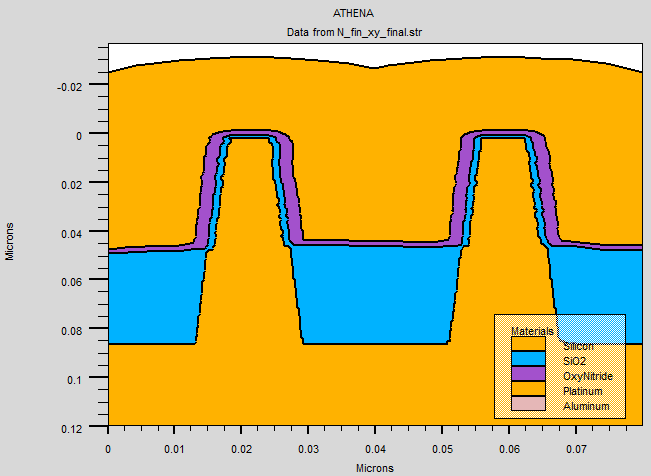
Fig 2.18 cross section view of completed FinFET structure
Another layer of oxide is deposited surrounding fins using dry O2, followed by etch of corner to remove sharp edges. Next, thin gate oxide layer is despite, followed by the deposition of dielectric layer and metal gate. Silicon oxynitride is use as the second dielectric on top of the oxide and platinum is used as the metal gate. Lastly, gate electrode is created for the gate and bulk. The resulting fins are 12nm in length with a 28nm separation between fins showing in figure 2.18.
2.3 Silvaco Simulation Comparison

Fig 14. Logarithmic (Red) and Linear (Green) plot of subthreshold current of N-channel FinFET
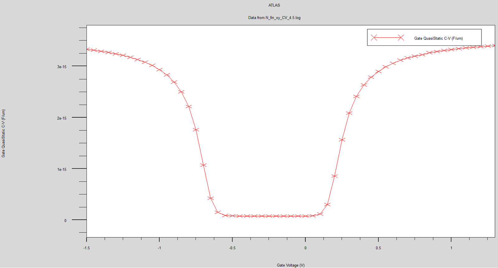
Fig 15 Gate capacitance sweep of N-channel FinFET
The device simulated has a workfunction of 4.5 C-V with doping of 1E18 using arsenic. The drain voltage is fixed at 0.1V. The Fin dimension is 40nm in height and 10nm in Length. Since the simulation is only 2 dimensional for the top of fins, a downward shift of 0.09 for the plot is required to account for the sides.
Given those simulation conditions, the Sub-threshold swing (SS) is 80 mV/decade, Threshold voltage is 0.45 V, and the leakage current is low at 2E-17 A. For the gate capacitance shown in figure, the peak gate capacitance is around 3.3E-15 F/um2.

Fig 16. Logarithmic plot of subthreshold current for both FinFET and bulk CMOS [11]
In order to validate the simulated result obtained using Silvaco, a similar FinFET simulation [using HSPICE and Predictive technology models (PTMs)] with slightly different process and dimensions are used as comparison. The compared FinFET Lg of 24nm, EOT of 1.1 nm, Tfin of 15nm, Hfin of 28nm and source/drain doping of 3E26 cm-3. Furthermore, a separate Bulk CMOS with 71nm in width and 22nm in gate length is also plotted as comparison. [11]
The HSPICE simulation FinFET has SS of 71 mV/decade at VDS of 0.1V, which is about 21% lower than the bulk CMOS using similar technology note. Interestingly, the SS of compared FinFET is about 12% lower than the FinFET simulated using Silvaco. This is likely due to the doping concentration of source/drain, which is much higher in comparison, despite the differences in fin length and height. On the other hand, Figure xx also shows a much better SCE suppression than bulk CMOS in term of DIBL.

Fig 17. Logarithmic plot of subthreshold current for SOI FinFET [12]
On the other hand, the simulated Bulk FinFET is compared to a separate SOI FinFET for similarities. The simulated of SOI FinFET has gate length of 20nm, width of 10 nm, and EOT of 2.1nm. Tfin of 10nm, Hfin of 40nm, and S/D doping of 2E18 cm-3. The SS for SOI NMOS and PMOS is at 75 mV/decade and 90 mV/decade respectively, which is very similar to the bulk FinFET simulated using Silvaco.

Fig 18. Logarithmic plot of subthreshold current for SOI FinFETs and Bulk FinFETs [12]
Lastly, the bulk Silvaco FinFET gate capacitance result is compared to both SOI FinFETs and Bulk FinFET with similar fin dimensions. First, the peak gate capacitance for the SOI FinFET with buried oxide thickness of 3000nm is identical to that of bulk FinFET in figure 18. Secondly, it can be observed that as the thickness of the BOX decreases, the gate capacitance increases slightly. While the gate capacitance differences are small in comparison to BOX thickness at the inversion region, the author suggested that this differences will become much more signification at depletion region [12].
In comparison to the bulk FinFET in figure 15 using Silvaco, the gate capacitance of SOI FinFET at the inversion region is relatively small. However, as the gate voltage approaches the depletion region, the gate capacitance of SOI FinFET saturates around 30 aF/cm2, while the bulk FinFET capacitance in figure 15 approaches almost zero toward the depletion region.
Additionally, the gate capacitance of bulk FinFET is equivalent to that of SOI FinFET with BOX thickness exceeding 3000 nm, which can be observed in figure 18. However, it is generally not desired to have thick BOX in SOI FinFET, due to heat dissipation problem(that will be discussed in section 3.1). Therefore, bulk FinFET in general has a lower gate capacitance than SOI FinFET with thin oxide. [12]
While it is difficult to have a direct comparison between three different FinFET with multiple different variables and processes, one can still conclude that the FinFET in general has a much better SCE suppression and lower SS over bulk planar MOSFET. Most importantly, despite the lower Fin length and larger Fin height of Silvaco FinFET in figure, it did not produce a smaller SS as result. This suggest that other parameters, in addition to fin thickness, also play a large role in determine the SS overall.
3 Discussion
3.1 Self-heating
Self-Heating Effect (SHE) is one of the disadvantages of FinFET, especially SOI FinFET with reduced bottom oxide. While planar bulk MOSFET also suffers SHE as result of phonon boundary scattering, due to the structure of FinFET, the effect of SHE is more sever in most cases [13]. On the other hand, while bulk FinFET has a greater degree of freedom in term of SHE mitigation, the problem still exists. Therefore, it is important to model and exam the effects of SHE for FinFET in analog design, where temperature plays a much bigger role.
Similar to bulk planar MOSFET, BTI (Bias Temperature Instability) characterization is used to obtain the effect of temperature on FinFET by stressing the FinFET with higher than nominal gate bias voltage, while the effects on multiple parameters are recorded. The amount of stress can be controlled by either magnitude or duration of the gate voltage applied.
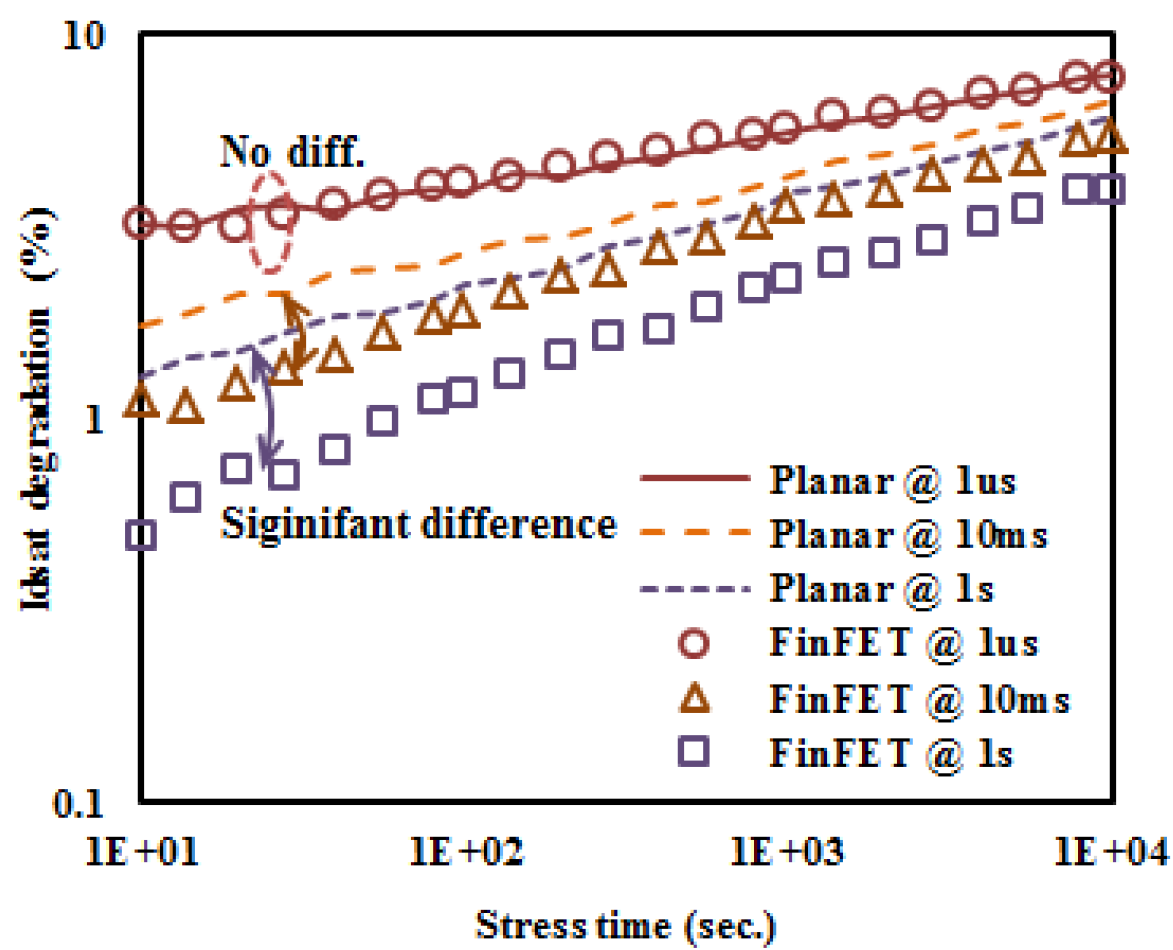
Figure 19. Drive Current degradation vs. stress time at difference measurement delay for Planar and FinFET
Using a 16nm node bulk FinFET as a test platform, Dr. S. E. Liu from TSMC was able to demonstrated the difference between planar and FinFET in term of saturation current degradation when plotted against duration of thermal stress exposed. It can be observed from figure 19 when measurement delay exceeding 10ms, significant differences are shown in term of saturation current degradation for FinFET toward the lower spectrum of stress time. On the other hand, as the stress time increases with reduced delay, the difference in saturation current shrinks between FinFET and Planar Bulk MOSFET. This result demonstrates the disadvantage of FinFET in term of recovery effects, which can be overcome be either restricting the delay time or threshold shift [13].

Figure 20. Cross sectional view of simulated (a) Bulk FinFET and (b) SOI FinFET [14]
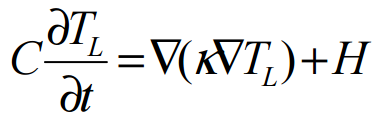
The effect of SHE can be more clearly observed though the more familiar IV plots. The simulation of IV plots without and without SHE is conducted by a group of researchers from the University of Bangladesh [14]. To start, the SHE is simulated by incorporating the lattice heat flow equation (in appendix 3.7) into the 3D Schrodinger-Poisson equation, which takes into the effect of thermal conductivity and heat capacitance [14]. The simulated dimension for Bulk FinFET is 30nm for gate length, 10nm for fin width, 15nm for fin height, 3nm for gate thickness(shown in figure 20 a). The SOI FinFET contains the identical dimension, expect with the additional buried oxide of 10 nm wide and 20nm thick (shown in figure 20 b).

Figure 21. Comparison of SHE though IV plot for Bulk FinFET at multiple gate voltages
Starting with Bulk FinFET, in figure 21, it can be observed that the drain current with the SHE tends to decrease with increase in Drain voltage for gate voltage higher than 1.1V. On the other hand, at gate voltage of 1.1V, the sweeping of Drain voltage does not produce a differences between SHE and non-SHE drain current.

Figure 22. Comparison of SHE though IV plot for SOI FinFET at multiple gate voltages
In comparison with Bulk, the effect of SHE on SOI FinFET is much greater. It can be observed in figure 22 that the degradation of drain current is very server for gate voltage exceeding 1.1V. More specifically, the additional silicon-dioxide layer under the channel and S/D region does not conduct heat very well.
In term of SHE, based on the presented results, Both SOI and bulk FinFET have more severe drive current degradation in comparison with planar MOSFET. However, the effect of SHE can be reduce with thinner layer of buried oxide for SOI FinFET, which also increases the gate capacitance , as it was stated in section 2.3. Yet, reduction of buried oxide thickness does have negative consequences, and the comparison between thin and thick buried oxide will be presented in section 3.2.
3.2 Thick vs Think BOX in SOI FinFET
SOI FinFET can be further divided into two categories of thick SOI FinFET and think SOI FinFET based on burred oxide thickness (BOX). In short, while there are advantages and disadvantages to both thick and thin BOX SOI FinFET, thick BOX SOI FinFET is considered to be superior based scalability and other design parameters [14].

Figure 23. Thick box SOI FinFET [14
The comparison of thin and thick BOX FinFET presented in this section is based on the simulation results presented Dr. Trivedi from the University of Florida. To start, the advantage of and disadvantage of thin BOX FinFET in comparison to thick can be summarized as the following:
- Advantage:
- Better SCE Control due to high electric field
- Better heat dissipation
- Disadvantage:
- Degraded carrier mobility/current due to high electric field
- Increase S/D Junction & body capacitance
- Result in degradation of switching speed
Starting with SCE control, this is directly related to the thin BOX’s higher gate capacitance previous discussed in section 2.3 of this report. More specifically, higher gate capacitance allows for better coupling of the gate, which allows the gate voltage to control the inversion channel better.
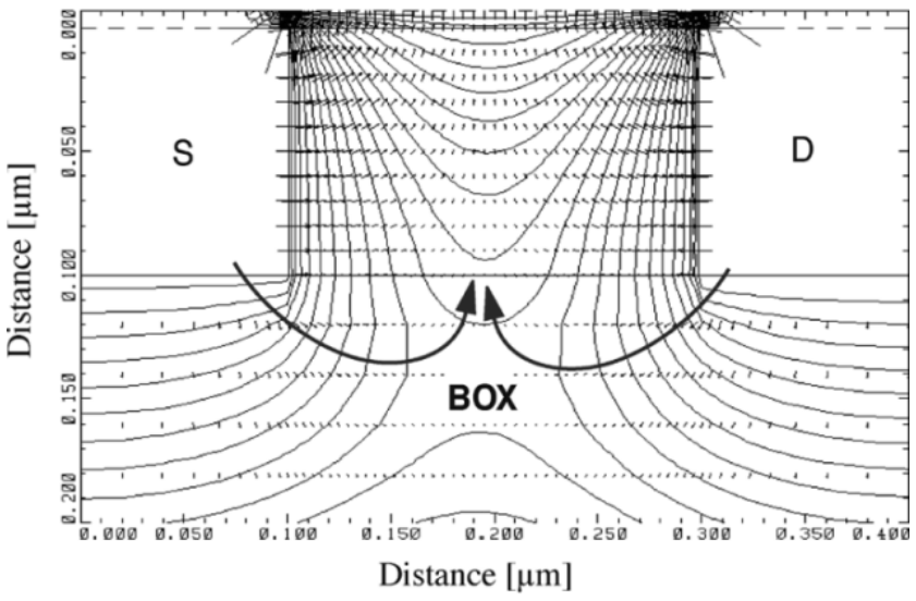
Figure 24. Electric field vectors shows the effect of filed fringing in BOX [14]
The effect SCE in thick BOX can be explained though the effect of electric-field fringing. For thick BOX, the effect of electric-field fringing can be visually observed in figure 24, (based on Leff of 0.2 um, silicon thickness of 100nm, BOX of 350nm and VDS of 50 mV,) as large amount of electric field terminates in the SOI body, the effect of SCEs due to 2-D effects of SOI body is amplified, in addition to augmenting subthreshold current [14].
To overcome the effect of electric-field fringing, thinning of BOX down to the scale of 25 nm is needed (depending on the silicon thickness). However, the difficulty in producing thin BOX is related to defect density, and alternatives to traditional SIMOX process is needed [14].
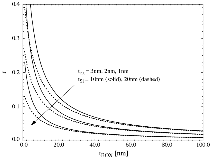

Figure 24. (a) Electric field vectors shows the effect of filed fringing and (b) transverse electric field with respect to change in BOX
On the other hand, reducing BOX causes increase in gate-substrate charge coupling factor, which can be observed in figure 24 a. Gate-substrate charge coupling will affect both the long-channel state swing and on sate current, therefore degrades the performance of SOI FinFET. This degradation is further amplified by reduction on carrier mobility (as result of the high ExC illustrated in Figure 24 b). Lastly, Dr. Trivedi referenced another research [15] regarding the augmentation of CJS/D, which reduces the operational speed of CMOS by as much has 20% in comparison to thick BOX CMOS.
3.2 FinFET under Low Temperature operation
Low temperature electronics is an important part of analog devices in modern society, its application ranges from infrared detectors to terrestrial applications. For example, some of the applications for low analog devices are space operations, satellite communication, magnetic levitation transportation system, medical diagnostics, cryogenic instrument, and superconductive magnetic energy storage system [16]. Most importantly, while it is desirable to reduce thermal stress for FinFET, FinFET at low operational temperature also brings other desirable characteristics for FinFET.
It is well established that planar bulk MOSFET under low temperature exhibit multiple enhanced characteristics, including faster operation speed, saturation velocity, carrier mobility (lower parasitic resistance). However, since the limitation of planar bulk CMOS scaling has been reached, further scaling of low temperature analog device requires the utilization of alternative technologies such as FinFET.
In a research published by Dr. Nandi, Saxena and Dasgupta from IIT Roorkee, a detail comparison of high-k and dual-k spacer FinFETs shown very promising performance for underlap FinFET with dual-k spacer under low temperature. The simulation is performed using gate length of 16nm, fin width of 8 nm, oxide thickness of 1.1nm and VDS of 1.1 V.


Figure 25. (a) gm and gds and (b) gm /Ids ratio with respect to normalized drain current [16]
From figure 25, it can be observed that high-k gate dielectric is unsuitable for low analog FinFET devices, due to the decrease of dc gain with respect to dielectric constant. More specifically, dielectric constant of the gate dielectric causes increase in fringe-induced barrier lower, resulting in lower DC gain.
In summary, based on the simulation results, dual-k spacer-based FinFET under low temperature is a promising alternative to planar bulk MOSFET, due to the lower dielectric constant of the gate dielectric that reduces the effect of fringe-induced barrier lowering, therefore allowing for a higher DC gain, cutoff frequency, and maximum oscillation frequency [16].
3.3 Parasitic capacitance and resistance
Two major challenges in the adoption of FinFETs for analog devices is related to the parasitic capacitance and resistance in both SOI FinFETs and Bulk FinFETs. Parasitic resistance refers to contact and diffusion/extension region resistance of source/drain while capacitance refers to the gate and junction capacitance. Parasitic has a large effect on current drive while parasitic capacitance has a large effect on the operation speed of FinFET.


Fig. 26. of 14 nm bulk FinFETs versus interfacial contact resistivity using metal contact area of (a) 30 x 30 nm2 and (b) 40 x 40 nm2 [17]
Starting with parasitic interfacial resistance, it has a huge impact on current drive and transconductance for FinFETs. Similar to MOSFET, one way to decrease parasitic interfacial contact resistance is though the increase in contact area. The comparison of drive currents between two different contact designs can be seen in figure 26. Given a much larger contact area of 40 x 40 nm2 for both source and drain in Figure 26 (b), the drive current is clearly superior to FinFET with smaller source/drain contact areas. [17]
FinFET could operate with undoped channel, which has its advantage in suppression of SCE and doping introduce defects/fluctuations. However, due to parasitic resistance, especially in the extension/diffusion regions of FinFET, extension doping is oftenly required for high performance FinFETs.
The doping of extension region is complicate by the fin height, which prevents the dopant from reaching the extension region at a vertical angle. As result, extension doping require a highly titled implant angle, in order to access the extension region thought its sidewalls. As result, angled extension implant is required for the formation of uniform extension regions. More specifically, because the extension region of FinFETs is orthogonal to wafer normal, a highly angled implant would be much more effective in achieving unformed extension regions [17].

Fig. 27 Extension resistance versus fin thickness for two doping types
FinFETs extension resistance is closely tie to Fin Thickness, in additional to dopant species. For example, based on figure 27, FinFETs with Fin Thickness smaller than 25nm shows a signification increase in extension resistance. As result, the implant of extension region for FinFET is an important steps in scaling FinFETs [17].

Fig. 28 Drain current versus drain voltage for PMOS and NMOS with and without RSD & silicide [17]
The reduction of parasitic resistance can also be achieved through raised source and drain (RSD) and silicide forming. First, because of the lack the deep source and drain regions in FinFETs, two separate techniques are required in formation of silicide contacts for FinFETs, which are low barrier silicide, or increasing thickness of fin outside the gate region with silicon epitaxy. From figure 28, it can be observed that given the identical Leff of 30 nm and silicon thickness of 20nm, FinFET with both RSD and silicide performances much better in turn of drive current. However, the performance gain in silicide for PMOS is not as noticeable, which the authors suggested is due to the RSD thickness on N-doped fins being significantly thinner [17].
Fig. 29 Transconductance versus Leff for <100> and <110> directed fins [17]
Additionally, using both NMOS and PMOS FinFETs with of 30 nm, of 20 nm, figure 29 shows FinFET with much shorter Leff has a much better transconductance. However, in term of fin directions, the performance gain for NMOS and PMOS varies. In figure 29, PMOS with <100> directed fins has a lower transconductance than <110> directed fins, while the opposite is true for NMOS.

Fig. 30 silicon epitaxy growth rates versus fin doping and orientation [17]
While the performance difference between <110> and <100> directed fins is not consistent, <100> directed fins holds the advantage in epitaxy growth rate. The importance of crystallographic in FinFET performances can be observed in figure 30. For example, above figure 30 indicates fins with <110> orientation has as much as twice the growth rate than FinFETs with <100> [17].
3.31 Geometry dependency of parasitic resistance
Geometry plays a major role in parasitic characteristics of transistor, especially for 3D based technology such as FinFET. While the 3D nature of FinFET makes it more challenging to design and simulate, it also gives analog designer more flexibility in optimizing parasitic resistance & capacitance. Therefore, this section will focus on the research results published by Dr. Pathak and Darji from the University of SVNIT in Surat, India regarding geometry dependence of source/drain parasitic for FinFET. (Please refer to appendix 4.3 for simulation parameter used.)
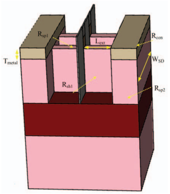
In the publication, the parasitic resistance between source and drain is divided into four sections, which are spread resistance (RSP1), sheet resistance (Rsh), spread resistance of highly HDD region (RSP2) and contact resistance (Rcon). (Parasitic resistance sections divided is visually illustrated in appendix 4.4.)


Fig 31. Parasitic resistance versus (a) Fin Height and (b) Fin Width [18]
To start, figure 31 has the most straightforward relationship between fin height and parasitic resistances, which shows the overall decrease in parasitic resistances in the S/D region with respect to increase in fin height and width. This includes the spread resistance, sheet resistance, and contact resistance.

Fig 32. Metal contact versus parasitic resistance [18]
In figure 32, the thickness of contact metal is plotted again spread resistance, contact resistance and lower resistance. Unsurprisingly, while lower resistance or spread resistance vary little to contact metal thickness; the reduction of contact resistance favors a much higher metal thickness to reduce parasitic [18].
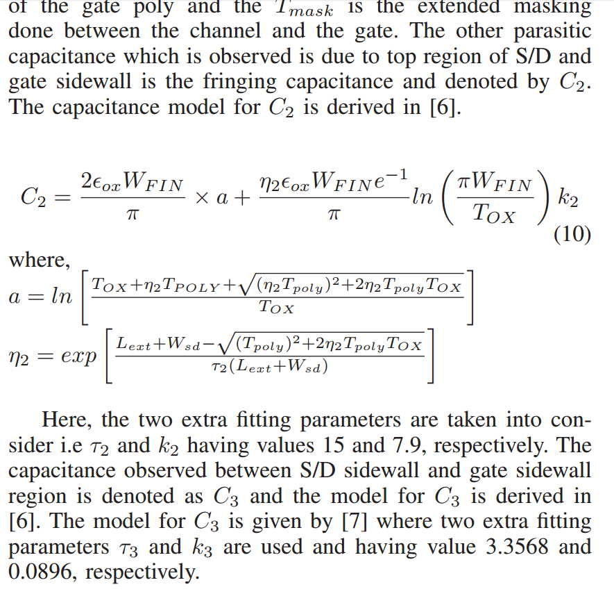
3.32 Geometry dependency of parasitic capacitance
High parasitic capacitance causes extensive intrinsic delay of FinFETs, which is especially problematic for RF analog circuits. There are total of three capacitances simulated by the authors, and their respective equations used for simulations are listed in appendix 3.9-4.1.
C1 (in appendix 3.9) is the fringing capacitance between the S/D the gate on the top of FinFET, (in appendix 4.0) is the capacitance between the top region of S/D and the gate sidewall, which accounts for two additional fitting values of , and (in appendix 4.0) is the capacitance between S/D sidewall and the gate sidewall, which accounts for two additional fitting values of . The variable representation in three parasitic capacitance equations is list in appendix 4.2.

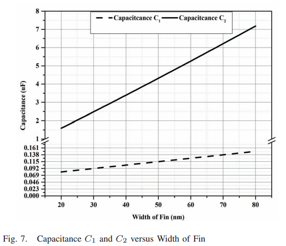
Fig 33. Parasitic capacitance (a) versus fin height (b) and fin width [18]
For parasitic capacitance, the most straightforward relationship is between the gate sidewall capacitate (C3) and sidewall of S/D region, which shows a positive learn relationship between Height of Fin and parasitic capacitance (in figure 33 (a)). On the other hand, Width of Fin also increases parasitic capacitances for the two other regions (C1 and C2) linearly, which is illustrated in figure 33 (b),. In summary, opposite to parasitic resistance, the reduction of parasitic resistance requires the reduction of fin height and fin width.
Based on above simulation results conducted by Jay and Darji from SVNIT, India, it is clear the reduction of parasitic capacitance and resistance requires careful balancing and prioritization. In general, while patristic resistance can be improved though increase in fin width and height, they also increase parasitic capacitive as result. As result, in additional to finding a fine balances on the width and height of fins, geometry manipulation of FinFETs should also take into account of the applications of device, and prioritize either capacitance or resistance based on its needs.
3.33 RF Performance

Fig 34 Effective gate to source voltage versus applied gate voltage with varying VDS voltage from 0V to 1.35V [19]
The negative effect of parastic capaictance & resistance is examed in this section using RF devices. To start, it can be observed in figure 34 that the actual effective gate source voltage versus applied gate source voltage varies depending on VDS. More specifically, when applied gate source voltage is at 1.2V, the effective gate source voltage is only at 0.9, and approximately 35% of voltage is lost to parasitic resistance.

Fig 36 Comparison of trans-conductance between FinFET and Planar FET with and without MG/HiK [19]
Secondly, when comparing FinFET against planar FET, it can be observed that FinFET trans-conductance drops significantly as drain a current increase, which is directly related to the negative side effect of series parasitic resistance in FinFET. More specifically, from figure 35, since the actually applied gate voltage drops significantly at higher VDS, it significantly degrades drain current as result, therefore negatively impact trans-conductance.

Fig 37. Peak cutoff frequency comparison between SOI FinFET and Planar FET with VDS at 1.2V [19]
Similarly, due to parasitic capacitance dsicussed in section 3.32, in term of high frequency applications, FinFETs will fundamentally lag behind plannar MOSFET. This can be observed in figure 37 when compared against planr bulk FET using intrinsic cutoff freuqnecy[19].
Lastly, the comparison of RF applicaiotn between SOI FinFETs and Bulk FinFETs can be summarized by reuslts presented by a group of researchers from University of Zagreb, Croatia. Using a 20 nm based gate length FinFETs, the comparisn between dopped and undoped FinFETs with SOI and BULK is summarized from two separate tables listed in appendix 4.6-4.7. More specifically appendix 4.7 details the perfroamce of cut-off and maxiumim freuqnecy between four separate FinFETs, while appendix 4.6 shows other analog parameters when comariing FinFET against eachother[1].
3.4 Random Telegraph Signal
It has been well established that random trapped charges on the gate oxide produces RTS (Random Telegraph Signal), which is a major source of noise in analog and RF circuits. Also referred to as burst noise, RTS is an electronic noise with similarity to low frequency digital signal. Its amplitude can range from microvolt to several millivolt. RTS is mainly generated by contamination of gate oxide by mobile charge carriers. RTS can be worsen by heavy ion implantation and other manufacturing processes. Further, RTS noise is especially dominate in short channel devices, which is a major concern as FinFET and other advanced technologies that continues to push for smaller gate lengths.
As mobile charge carriers passes through the channel, small amount of charges are trapped in the, either on the surface or inside the oxide. As the trapped charges charging and discharging during operation, a continuous electrical noise is generated. The variables that can affect RTS are columbic scattering effect, doping uniformity, doping concentration, temperature, and geometry of MOSFET.
The simulation of RTS as result of oxide defect can be accomplished for both linear and saturation region using Unified Number Mobility Fluctuation theory. This relationship is summruized in appendix

- W- Width channel
- L- Length of channel
- – charge density per unit area in the inversion layer
- µ-channel carrier mobility
- α- screened scattering coefficient.
The average µ in linear region is defined as the following
![]()
The average µ in saturation region is defined as the following:
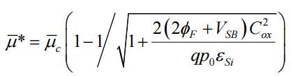
Equation in appendix xx indicates a strong correlation between RTS and the area of channel width and doping level. More specifically, smaller channel area will be more susceptible to RTS. Furthermore, channel carrier mobility is also a major contributor to RTS, which further exacerbate the noise level on short channel devices with heavy doping.
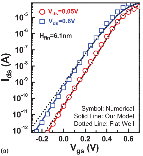
On the other hand, the characterization of RTS of small scale FinFET is published in 2015 by group of researchers from the institute of microelectronic in Singapore. In the experimental study, the authors used SOI FinFET with Si thickness of 200 nm on a 150nm BOX, while the fins have width of 70 and effective fin heights of 100 and 200nm. This gives the device an effective channel area of 0.02 um^2 with Vth of -0.15, subthreshold slope of 80 mV/dec and Ion/Ioff ratio of 10^6. (20)
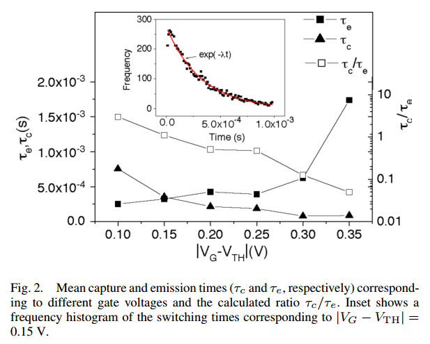
Fig 38. Mean capture and emission time for PMOS FinFET [21]
The mean capture and emission time in relationship to different gate votlage indicates the strong correlation between gate voltage and capture/emission time ratio. As the gate votlage increases, the trap occupancy time increases. The expoetinal relationship between freuqnecy and time correspond to a Poisson random process, which suggest that interface states is largely responsible for above results, therefore points to a strong correlation between quanlity issue of Si-SiO2 interface on FinFET and RTS [21].
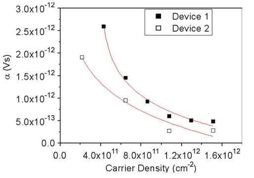
Fig 41. Scattering coefficient with respect to RTS amplitudes for single (device 1) and multi (device 2) active interface traps [21]
Because of the collreation between scattering coefficient and RTS, above graph shows a relatveion high RTS with respect to finFET carrier density. Since typical double lateral channel FinFET has hole mobility valvues of 10-50 cm^2/Vs, the range of scattering ofecicent is higher typical plannar MOSFET with with larger channel length.
The above experimental results indicated the strong relationship between scaling of SIO PMOS FinFET and higher RTS than conventional MOSFETs, which creates a hurdle for the extreme scaling of FinFET.


Fig 42. Average gate voltage noise of CMOS FinFET with respect to (a) drain current and (b) gate voltage [22]
On the other hand, RTS in CMOS FinFETs can be reduced though novel methods, such as anneling using hydrogen. This is demonsrtaed by Dr. Lee from the unversity of Texas, Richardson. From figure 42, it can be observed that the overall average gate votlage noise of CMOS FinFET is reduced with hydrogen annealing than CMOS FinFETs without.

Fig 43. Subthreshold characteristic of NMOS and CMOS FinFET without and without hydrogen annealing [22]
In summary, with hydrogen annealing, saturation current increases by as much has 30% for FINFETs, while low frequency noise level decreases drastically across all operation regions [22]. The overall improvement FinFET performance can be observed in figure 43. As result, hydrogen annealing a very processing enhancement/improvement process FinFET, in additional to reducing RTS.
3.5 Gate Fringe-Induced Barrier Lowering
While majority of the FinFETs studied are overlap based FinFETs, FinFETs with underlapped channel has shown promising results in term of Ion/off ratio and device delay. For example, in section 3.2 of this report, underlap FinFET shows an improved drive current under low temperature.
To further assess the advantage of underlap FinFET, this section will exam the publication presented by a group of researchers from the technical instituted of Mumbai regarding GFIBL and undoped underlap FinFETs. In summary, the results published shows significant improvement to both Ion/off ratio and device delay with respect to change in underlap length and dielectric constant.
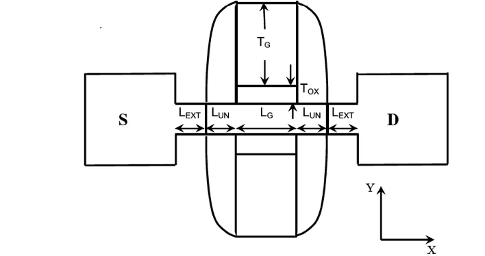
Fig 44. Top view of FinFET show underlap FinFET structure [23]
The experimental result is based on the simulation of 2-D FinFET structure using Sentaurus design suit that takes into account of density-gradient quantum correction, drift-diffusion mobility, and band tunneling. The structure has channel length of 20nm, effective oxide thickness of 0.75 nm. The underlap length is equivalent of channel length while the gat-electrode thickens is at twice the channel length.

Fig 45. On current gain in comparison to underlap length [23]

Fig 46. On current gain in comparison to underlap length [23]
Starting with Ion/off ratio, it can be observed in figure 45 that Ion/off ratio peaked around underlap length of 12nm. The improved in Ion/off ratio is result of GFIBL, which can be correlated to result in figure 46. Using two gate-electrode thickness of 40nm and 2nm, the differences in Ion with respect to change in underlap length is result of GFIBL. As the underlap length decreases to 0, the differences between Ion vanishes, and so does GFIBL.
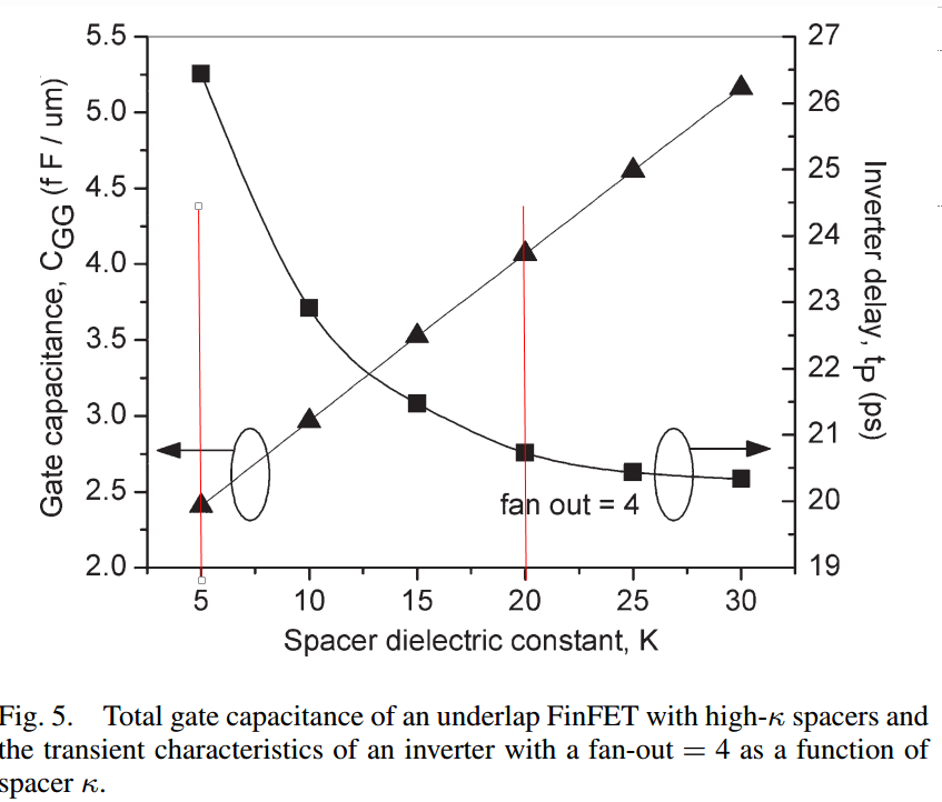

Fig 47. Capacitance and on current versus Spacer dielectric constant K [23]
Furthermore, in additional to optimization underlap length, spacer dielectric constant K is also another parameter that can be optimized. The importance of dielectric constant K can be observed in figure 47 for both gate capacitance and saturation current. In short, it can be sobered that deictic constant K of around 20 is ideal, which shows the minimum amount of delay and maximum On/Off current ratio.
The use of un-doped underlap regions are especially useful for scaled down FinFETs, as the process variation of doping profiles for finer fins are much more difficult to predict and control. Most importantly, the performance of FinFET can be further improved by utilizing high dielectric constant K with spacers.
4 Conclusion
As semiconductor industry continues to chasing Moore’s law, it is no longer feasible to further reduce the length of the gate below 28nm using the traditional bulk planar MOSFET, due to Short Channel Effect (SCE). More specifically, as the gate continues to shrink, its ability to control the conducting channel continues to decrease, result in many undesired effects in short channel devices.
In summary, FinFET is a promising replacement for MOSFET in the digital world, mainly for digital system’s ability to take the full advantage of superior SCE suppression FinFET offers. However, in the world of analog, given the advantages and disadvantage of FinFET, it may not be a viable route for the analog industry.
To start, Self-Heating Effect (SHE) is one of the disadvantages of FinFET, especially SOI FinFET with reduced bottom oxide. While thick oxide offers many advantages, including better suppression of SCE, SHE limits the thickness of SOI in FinFET, depending on operation temperature. On the other side of the spectrum, thin SOI FinFET is haunted by other problems, including cost per wafer, defect density of BOX, and complicate designs.
Most importantly, the challenges that face analog designers can be very different than what digital designer faces, which further complicate the adoption of FinFET. For example, based on the fundamental nature of FinFET structure, SOI and bulk FinFET will always lag behind bulk planar MOSFET in term of pure cut-off frequency and switching delays due to parasitic capacitance.
On the other hand, while there are many challenges in adoption of FinFET for analog systems, there are also many promising solutions. For example, parasitic capacitance and resistance can be reduced though the careful design of FinFET geometry, random noise can be suppressed though the use of hydrogen annealing, and SCE suppression can be further improved with the use of underlap FinFET in combination of high dielectric K.
In conclusion, there are still many challenges face the adoption of FinFET for analog devices. While there may not be an immediate advantage in switching to FinFET for analog devices, as the adoption of FinFET for digital slowly matures, the differences between FinFET and MOSFET will eventually shrink overtime for certain analog applications. In the end, there will always be advantages to MOSFET that FinFET cannot replace, just as the advantages to BJT that MOSFET can’t replace, and the adoption of FinFET for analog systems may never be as clear as one may expect them to be
Appendix
(Appendix 2.1)

(Appendix 2.11)
(Appendix 2.12)

(Appendix 2.2)
| Cut Off | ||
| Linear | ||
| Saturation |
(Appendix 2.3)
| Cut Off | ||
| Linear | ||
| Saturation |
(Appendix 2.4)
 Linearly Region
(Appendix 2.5)
 Saturation Region
(Appendix 2.6)
 Subthreshold Region
(Appendix 2.7)
 2nd order Poisson equation
(Appendix 3.1)
 Sheet charge TG FinFETs
(Appendix 3.2)
 Sheet charge DG FinFETs
(Appendix 3.3)
(Appendix 3.4)
(Appendix 3.5)

(Appendix 3.6)


(Appendix 3.7)

(Appendix 3.8)
(Appendix 3.9)

(Appendix 4.0)
(Appendix 4.1)

(Appendix 4.2)
- = Gate Extension
- = Fin Width
- = Dielectric Permittivity
- = Gate Length
- = Thickness of Gate Poly
- = Thickness of Extended Mask
(Appendix 4.3)

(Appendix 4.4)
(Appendix 4.5)

(Appendix 4.6)

(Appendix 4.7)

(Figure 1.2)
Figure xx S. H. Wu, C. L. Yu, C. H. Yu and P. Su
 (2.11)
References
[1] S. Krivec, H. Prgić, M. Poljak and T. Suligoj, “Comparison of RF performance between 20 nm-gate bulk and SOI FinFET,” 2014 37th International Convention on Information and Communication Technology, Electronics and Microelectronics (MIPRO), Opatija, 2014, pp. 45-50.
[2] Graef, Mart, International Technology Roadmap for Semiconductors 2005 Edition – Executive Summary, www.itrs.net.
[3] G. E. Moore, “Cramming More Components Onto Integrated Circuits,” in Proceedings of the IEEE, vol. 86, no. 1, pp. 82-85, Jan. 1998.
[4] S. Das and S. Kundu, “Simulation to Study the Effect of Oxide Thickness and High- K Dielectric on Drain-Induced Barrier Lowering in N-type MOSFET,” in IEEE Transactions on Nanotechnology, vol. 12, no. 6, pp. 945-947, Nov. 2013.
[5] Fuller, Lynn Phd. “The Short Channel MOSFET “MCEE 732 Microelectronics Manufacturing. Rochester Institute of Technology, n.d. 07 Apr. 2017. pp. 6-7.
[6] K. Yamasaki and M. Hirayama, “Determination of effective saturation velocity in n+self-aligned GaAs MESFET’s with submicrometer gate lengths,” in IEEE Transactions on Electron Devices, vol. 33, no. 11, pp. 1652-1658, Nov 1986.
[7] Yuan Taur, Xiaoping Liang, Wei Wang and Huaxin Lu, “A continuous, analytic drain-current model for DG MOSFETs,” in IEEE Electron Device Letters, vol. 25, no. 2, pp. 107-109, Feb. 2004.
[8] H. C. Pao and C. T. Sah, “Effect of diffusion current on the device characteristics of insulated-gate field-effect transistors,” in IEEE Transactions on Electron Devices, vol. 12, no. 9, pp. 509-509, Sep 1965.
[9] A. Tsormpatzoglou, N. Fasarakis, D. H. Tassis, I. Pappas, K. Papathanasiou and C. A. Dimitriadis, “Analytical unified drain current model of long-channel tri-gate FinFETs,” 2012 28th International Conference on Microelectronics Proceedings, Nis, 2012, pp. 115-118.
[10] D. S. Havaldar, G. Katti, N. DasGupta and A. DasGupta, “Subthreshold current model of FinFETs based on analytical solution of 3-D Poisson’s equation,” in IEEE Transactions on Electron Devices, vol. 53, no. 4, pp. 737-742, April 2006.
[11] H. Farkhani, A. Peiravi, J. M. Kargaard and F. Moradi, “Comparative study of FinFETs versus 22nm bulk CMOS technologies: SRAM design perspective,” 2014 27th IEEE International System-on-Chip Conference (SOCC), Las Vegas, NV, 2014, pp. 449-454.
[12] Lee, J.H.: Bulk FinFETs: design at 14 nm node and key characteristics. In: Kyung, C.-M. (ed.) Nano Devices and Circuit Techniques for Low-Energy Applications and Energy Harvesting. KAIST Research Series, pp. 50–56. Springer, Dordrecht (2016)
[13] S. E. Liu et al., “Self-heating effect in FinFETs and its impact on devices reliability characterization,” 2014 IEEE International Reliability Physics Symposium, Waikoloa, HI, 2014, pp. 4A.4.1-4A.4.4.
[14] V. P. Trivedi and J. G. Fossum, “Nanoscale FD/SOI CMOS: thick or thin BOX?,” in IEEE Electron Device Letters, vol. 26, no. 1, pp. 26-28, Jan. 2005.
[15] P. C. Yeh and J. G. Fossum, “Physical subthreshold MOSFET modeling applied to viable design of deep-submicrometer fully depleted SOI lowvoltage CMOS technology,” IEEE Trans. Electron Devices, vol. 42, no. 9, pp. 1605–1613, Sep. 1995.
[16] A. Nandi, A. K. Saxena and S. Dasgupta, “Enhancing Low Temperature Analog Performance of Underlap FinFET at Scaled Gate Lengths,” in IEEE Transactions on Electron Devices, vol. 61, no. 11, pp. 3619-3624, Nov. 2014.
[17] J. Kedzierski et al., “Extension and source/drain design for high-performance FinFET devices,” in IEEE Transactions on Electron Devices, vol. 50, no. 4, pp. 952-958, April 2003.
[18] P. Jay and A. D. Darji, “Analysis of the source/drain parasitic resistance and capacitance depending on geometry of FinFET,” 2015 11th Conference on Ph.D. Research in Microelectronics and Electronics (PRIME), Glasgow, 2015, pp. 298-301.
[19] V. Subramanian et al., “Planar Bulk MOSFETs Versus FinFETs: An Analog/RF Perspective,” in IEEE Transactions on Electron Devices, vol. 53, no. 12, pp. 3071-3079, Dec. 2006.
[20] M. A. Nour et al., “A scalable random telegraph signal simulation based on experimentally — Identified gate oxide defects,” 2015 International Conference on Noise and Fluctuations (ICNF), Xian, 2015, pp. 1-4.
[21] Y. F. Lim et al., “Random Telegraph Signal Noise in Gate-All-Around Si-FinFET With Ultranarrow Body,” in IEEE Electron Device Letters, vol. 27, no. 9, pp. 765-768, Sept. 2006.
[22] Jeong-Soo Lee, Yang-Kyu Choi, Daewon Ha, S. Balasubramanian, Tsu-Jae King and J. Bokor, “Hydrogen annealing effect on DC and low-frequency noise characteristics in CMOS FinFETs,” in IEEE Electron Device Letters, vol. 24, no. 3, pp. 186-188, March 2003.
[23] A. B. Sachid, C. R. Manoj, D. K. Sharma and V. R. Rao, “Gate Fringe-Induced Barrier Lowering in Underlap FinFET Structures and Its Optimization,” in IEEE Electron Device Letters, vol. 29, no. 1, pp. 128-130, Jan. 2008.
[332]Lee, J.H.: Bulk FinFETs: design at 14 nm node and key characteristics. In: Kyung, C.-M. (ed.) Nano Devices and Circuit Techniques for Low-Energy Applications and Energy Harvesting. KAIST Research Series, pp. 50–56. Springer, Dordrecht (2016)
[332]H. Farkhani, A. Peiravi, J. M. Kargaard and F. Moradi, “Comparative study of FinFETs versus 22nm bulk CMOS technologies: SRAM design perspective,” 2014 27th IEEE International System-on-Chip Conference (SOCC), Las Vegas, NV, 2014, pp. 449-454.
[331]L. Chang et al., “Extremely scaled silicon nano-CMOS devices,” in Proceedings of the IEEE, vol. 91, no. 11, pp. 1860-1873, Nov 2003.
Bin Yu et al., “FinFET scaling to 10 nm gate length,” Digest. International Electron Devices Meeting,, San Francisco, CA, USA, 2002, pp. 251-254.
[13]”2003 Symposium on VLSI Technology. Digest of Technical Papers (IEEE Cat. No.03CH37407),” 2003 Symposium on VLSI Technology. Digest of Technical Papers (IEEE Cat. No.03CH37407), Kyoto, Japan, 2003, pp. .
doi: 10.1109/VLSIT.2003.1221057
(7) Yuan Taur, Xiaoping Liang, Wei Wang and Huaxin Lu, “A continuous, analytic drain-current model for DG MOSFETs,” in IEEE Electron Device Letters, vol. 25, no. 2, pp. 107-109, Feb. 2004.
P. Jay and A. D. Darji, “Analysis of the source/drain parasitic resistance and capacitance depending on geometry of FinFET,” 2015 11th Conference on Ph.D. Research in Microelectronics and Electronics (PRIME), Glasgow, 2015, pp. 298-301.
J. Kedzierski et al., “Extension and source/drain design for high-performance FinFET devices,” in IEEE Transactions on Electron Devices, vol. 50, no. 4, pp. 952-958, April 2003.
doi: 10.1109/LED.2003.809526
Y. F. Lim et al., “Random Telegraph Signal Noise in Gate-All-Around Si-FinFET With Ultranarrow Body,” in IEEE Electron Device Letters, vol. 27, no. 9, pp. 765-768, Sept. 2006.
doi: 10.1109/LED.2006.880640
S. Singh, S. S. Gill and N. Kaur, “Analysis of influence of temperature on 20nm triangular bulk FinFET,” 2016 IEEE International Conference on Recent Trends in Electronics, Information & Communication Technology (RTEICT), Bangalore, 2016, pp. 985-987.
S. H. Kim and J. G. Fossum, “Design Optimization and Performance Projections of Double-Gate FinFETs With Gate–Source/Drain Underlap for SRAM Application,” in IEEE Transactions on Electron Devices, vol. 54, no. 8, pp. 1934-1942, Aug. 2007.
Kyung, Chong-Min. Nano Devices and Circuit Techniques for Low-energy Applications and Energy Harvesting. Dordrecht: Springer, CISS, 2016. Print.
X. Sun et al., “Tri-Gate Bulk MOSFET Design for CMOS Scaling to the End of the Roadmap,” in IEEE Electron Device Letters, vol. 29, no. 5, pp. 491-493, May 2008.
S. H. Wu, C. L. Yu, C. H. Yu and P. Su, “Theoretical Investigation of DIBL Characteristics for Scaled Tri-Gate InGaAs-OI n-MOSFETs Including Sensitivity to Process Variations,” in IEEE Journal of the Electron Devices Society, vol. 5, no. 1, pp. 45-52, Jan. 2017.
P. G. Der Agopian, J. A. Martino, R. Rooyackers, A. Vandooren, E. Simoen and C. Claeys, “Experimental Comparison Between Trigate p-TFET and p-FinFET Analog Performance as a Function of Temperature,” in IEEE Transactions on Electron Devices, vol. 60, no. 8, pp. 2493-2497, Aug. 2013.
A. Wang, V. Dhawan and C. J. R. Shi, “Analog building block design in 14nm FinFET using inversion coefficient,” 2014 SOI-3D-Subthreshold Microelectronics Technology Unified Conference (S3S), Millbrae, CA, 2014, pp. 1-3.
E. Contreras, T. Granados-Luna, G. G. Pérez-Sánchez, R. Rodríguez-Figueroa and O. G. Serrano, “FinFET transistors for power analog circuits, analysis of harmonic distortion,” 2015 IEEE Workshop on Power Electronics and Power Quality Applications (PEPQA), Bogota, 2015, pp. 1-5.
J. Singh et al., “Analog, RF, and ESD device challenges and solutions for 14nm FinFET technology and beyond,” 2014 Symposium on VLSI Technology (VLSI-Technology): Digest of Technical Papers, Honolulu, HI, 2014, pp. 1-2.
S. K. Mohapatra, K. P. Pradhan, D. Singh and P. K. Sahu, “The Role of Geometry Parameters and Fin Aspect Ratio of Sub-20nm SOI-FinFET: An Analysis Towards Analog and RF Circuit Design,” in IEEE Transactions on Nanotechnology, vol. 14, no. 3, pp. 546-554, May 2015.
Colinge, Jean-Pierre. FinFETS and Other Multi-gate Transistors. New York: Springer, 2008. Print.
(5)Young-June Park, Ting-Wei Tang and D. H. Navon, “Monte Carlo surface scattering simulation in MOSFET structures,” in IEEE Transactions on Electron Devices, vol. 30, no. 9, pp. 1110-1116, Sep 1983.