

Abstract
This report is a summary of NIL (nanoimprint lithography). The topics include a brief history of NIL, the basic process steps for NIL, and the applications for NIL. The history of NIL includes patent research of the earliest NIL patents, the current NIL standing in terms of NGL (Next-Generation Lithography), and the pros and cons of NIL. The process for NIL is divided into two major processes of UV and thermal-based NIL, but skipped the mix of both UV-thermal processes many have adopted. The application including a brief list of deployed NIL applications and a bereft discussion of the antireflective coating application for NIL used in solar panels, lenses, LEDs, etc.
Index Terms—Nanoimprint lithography, hot embossing, Thermal NIL, UV NIL, photoresist, SWG, ITRS, NGL
Imprint Background/History
While the idea of plastic imprint has existed for decades, the most famous publication involving the use of polymer imprint for IC was introduced by Dr. Chou in 1995. More specifically, Dr. Chou demonstrated the first use of thermal nanoimprint lithography (NIL) for IC, and was able to achieve a strip length of 70nm with nearly perfect comers.
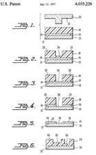
However, the first NIL publications for IC manufacturing belong to US patent 4,035,225 filed in 1977, followed by US patents 4,731,155 filed in 1988. In US 4,035,225, the inventors provided an illustration of hot embossing process in figure 1. On the other hand, in US patents 4,731,155 published in 1988, the author specifically stated the use of ‘embossed’ polymeric substrate for imprint lithography based on ‘pattern of peaks and valleys’ of the mold, and successfully created a feature in the nanometer range:
Regardless, there is a total of four claims by Dr. Chou in his patent filed in 1995. First, Dr. Chou stated that no one in the IC industry has recognized the use of molding to replace traditional optical lithography. Secondly, Dr. Chou stated that no method and apparatus were published on performing ultrafine patterns using molding. Third, giving the potential replacement to optical lithography, NIL has a huge utility. Lastly, Dr. Chou argued that NIL is a novelty, and the idea of imprint polymer for IC industry is new.
In patent 5772905, Dr. Chou further discussed the need for a more affordable technique in creating ultra-fine size patterns in the nanometer range, to reach the next to generate node more affordably during that time. Giving the fact that the patent was published in 1995 with target generation of 250nm, the IC industry was at a transition point between i-line and DUV lithography. Since 250nm is within the capability of both i-line and DUV, it is possible the desire for completely new lithography during 1995, such as NIL, was not high.
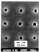
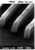
Nonetheless, during Dr. Chou’s time of publication, he was able to demonstrate the manufacturing of IC components based on NIL that well exceeded the capability of i-line generation in 1995. For example, in figure 2a, the contact hold has a diameter of 25nm and period of 120nm, which well exceeded the capability of i-line [1]. Furthermore, in figure 2b, the strip has a diameter of 70nm and height of 200nm, with impressive corners of nearly 90 degree [1]. Interestingly, Dr. Chou discussed NIL as a direct competition to x-ray lithography, and like many others, did not expect optical lithography to survive for as long as it did.
Giving the target generation node of 250nm in 1995, and the capability of NIL demonstrated by Dr. Chou, the author argued NIL was much more than an affordable technique for non-IC applications, but the lithography for IC going forward. More specifically, Dr. Chou argued that there wasn’t ‘an ongoing need’ in the IC industry to produce a smaller pattern size, but an urgent need to develop a low-cost technique for the mass production of ultrafine patterns alternative to optical lithography.
By 2003, because of the promising results demonstrated by Dr. Chou, NIL generated a large amount of interest in the R&D sector of IC manufacturing and received a surge of publications during that time. Most importantly, during 2003, International Technology Roadmap for Semiconductors (ITRS) even named NIL as one of the next-generation lithography (NGL) candidates.
However, technology such as NIL will not be able to materialize without the support and active funding from industry leaders, especially being such a disruptive technology with many unknowns at times. As result, in addition to putting NIL as NGL, ITRS also stated some of the remaining challenges (in 203) for NIL, including 1x mask, defect and overlay [2]. Some of the main challenges in adopting NIL for the replacement of optical lithography are [3]:
- NIL Process Requirement
- Because of the thermal and pressure requirement for thermal based NIL, it may not be compatible after certain metal layers, in addition to dopant disruption due to high thermal budget requirement.
- Stamp
- Degraded stamp can cause structure degradation, in addition to increase in defectivity.
- Throughput
- Thermal based curing significantly reduce the throughput of NIL, in additional to the need for new stamp.
- Overlay
- Overlaying an opaque stamp for thermal NIL within nanometer precision can be challenging on a manufacturing scale.
- Defectivity
- Since there is no optical reduction, NIL is more prone to stamp/mask imperfection that optical lithography can mitigate.
Today, after 20 years since the introduction of NIL by Dr. Chou, it is still unclear exactly what role NIL plays in the world of IC manufacturing. As the technology node continues to decrease, and continually improve in EUV, some may argue that NIL has lost its traction in the replacement of optical lithography for IC manufacturing. Giving the current target generation node of 7nm, and the additional optical lithography techniques introduced since 1995, including multiple patterning and immersion, the number of interests in NIL may have slowly faded for IC manufacturing.
However, giving the pros and cons of NIL, it is a perfectly suitable lithography technique for non-IC applications, especially in the manufacturing of nanometer structures with high tolerance to overlay of defectivity. Most importantly, the alternative to thermal NIL, such as UV NIL, has been introduced to overcome some of the initial challenges with NIL, which may potentially bring NIL back to ITRS roadmap again.
NIL Variation & Processes
After the work published by Dr. Chou, the amount of patents filed related to NIL has surged extensively, with many new innovative variations and implementation. Despite a large number of variations to NIL, the majority of those processes’ techniques can be categorized under two major groups of thermal and UV NIL.
Thermal NIL
Thermal NIL is the oldest NIL technique, and most thermal NIL presented today is very similar to the hot-embossing/thermal NIL technique introduced by S.Y. Chou in 1995. In short, thermal NIL uses heat and pressure to enable viscosity change during stamping. Under high pressure and temperature, the coated polymer on the substrate has a low viscosity, which allows it to fill into the gaps/structure of the stamp. With the stamp still pressed downward into the polymer, the polymer is allowed to harden again, which enables the solidification of features on the thin film.
Start with the patent filed by Dr. Chou, thermal NIL can be summarized in four major steps. Starting with the creation of the master mask using in the imprint, the author stated that the material chosen for the mold need to be harder than the thin film, and suggested that materials such as metals, dielectrics, semiconductor, and ceramic with the correct hardness can be used, depending on the thin film used for pattern transfer. The mold in the patent is using electron beam lithography and reactive ion etching.
The second step is the deposition of a transfer layer, which is made of PMMA that is spin-coated onto the wafer it ranges from 50 nm to 250 nm. PMMA was chosen by Dr. Chou for its non-adhesion to SiO2 mold, due to its hydrophilic surface, in addition to its thermal expansion properties [1].
Next, by pressing the mold made of SiO2 into the polymer above its glass transition temperature, the low viscosity of the polymer allows it to conform to the features of the mold. With the mold still inserted, the temperature is allowed to drop below the glass transition temperature, and the features imprint onto the PMMA solidifies. The ideal pressure and temperature stated by Dr. Chou during his experiment were at 200ºC and 1900 psi during imprint [1].
The biggest disadvantage in thermal NIL is its thermal and pressure requirement. Since it requires the use of high temperature and pressure, the process may damage the underneath structure. Secondly, depending on the surface area and temperature, the amount of pressure the stamp can apply without damaging the substrate can be a limiting factor to throughput, especially giving the fact thermal NIL polymer generally has a higher viscosity during stamping, even at elevated temperatures above its glass transition point.
One possible advantage to thermal NIL could is cost reduction. Giving the fact that the thermoplastic polymer used does not have to contain photon-sensitizer that is curable to radiation, there could be a potential cost advantage to the transfer pattern resist used for thermal plastic in comparison with UV.
UV NIL
Similar to thermal NIL, radiation energy is used instead of thermal energy to cure the pattern transfer resist, similar to the curing of PR under optical lithography. Instead of using heat to change the chemistry of the polymer in thermal NIL, UV-based NIL follows the approach of PR, and uses radiation instead to cure the polymer.
One immediate problem is the delivery of photon energy into the polymer. Since the polymer has to be cured during the stamp, it requires a transparent mask/stamp, in order to deliver the radiation through the stamp. Since absorbance increases with a decrease in wavelength, this requirement could potentially be a limiting factor to throughput and stamp/mask type.
In summary, depending on the type of mold being utilizing, UV NIL can be further divided into two categories of UV-NIL and Soft UV-NIL. To start, UV-NIL often refers to the use of quartz/glass as a stamp, while Soft UV-NIL uses soft/flexible polymeric stamp, such as PDMS, The advantages of soft UV-NIL includes flexibility, low interfacial free energy (∼21.6 dyn/cm), chemical stability and high optical transparency[4].
Mold
Most NIL process contains three major components; the master mold, the mold, and the pattern transfer resist. A master mold is comparable to the hard mask for optical lithography, which contains the patterns that NIL is trying to reproduce. However, since the ratio between mold and transferred pattern size is 1:1, the requirement for master mold is much more demanding, as there is no optical reduction and defocus of defects and imperfections.
As result, most high-resolution master molds are made of e-beam lithography and dry etch, while sallow master molds can be produced by e-beam lithography with metal life off [5]. The material chosen for master mold needs to exhibit smooth and straight features with low sidewall angles. Therefore, one of the most widely chosen materials for master mold is nickel [5]. Nickel fabricated by e-beam lithography and electroplating not only exhibits high resolution, smooth and straight features with low sidewall angles but is durable and hard [5].
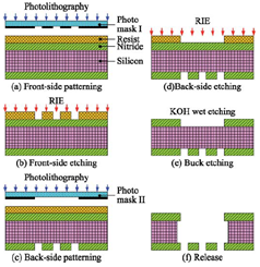
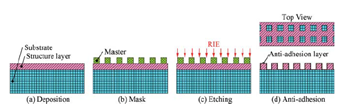
A novel approach to the fabrication of NIL master mold is the utilization of silicon nitride membrane and reactive ion etch. In summary, the process uses low-stressed silicon nitride to create a master mold with the pattern on one side and an opening on the other, separated by a thick layer of silicon [6]. This is then used as the master mold to transfer the pattern onto a replica mold by the use of reactive ion etch. The master mold is placed directly in contact with the replica mold layer, which acts as a hard mask during the dry etch that allows for the transfer of pattern onto the replica mold, illustrated in figure 3b extract from publication [6].
However since the fabrication of master mold requires the use of KOH(Potassium hydroxide) to remove the thick silicon layer between the low-stressed silicon nitride, the resulted master mold was often incomplete, due to membranes being broken off in the KOH wet process[6].
NIL Using PR
One approach to further reduce the cost of NIL is by utilizing preexisting PR technologies, instead of relying on the limited number of prosperity NIL resists with relatively high cost. Most importantly, the ability to utilizing the same PR for both imprint and optical lithography may bring additional advantages in design and cost.
Therefore, by tapping into cost-effective pattern transfer resist for NIL, such as PR with a relatively competitive pricing, multiple researchers have successfully demonstrated the use of optical PR as a viable nanoimprint resists with comparable performances.
The main challenges in finding a suitable PR for NIL are related NIL’s adhesion and thermal requirement. Because of the temperature requirement during NIL, for which the imprint temperature has to be above the glass transition temperature of the pattern transfer resist, most PRs would degrade overtime at a temperature above its glass transition. More specifically, PR would lose the majority of its photoactive component, which is directly tied to sensitivity and throughput. Secondly, PRs are optimized for adhesion, which could cause lifting of resist during decoupling of the mold from the PR after imprint.
Starting with the thermal effect on PR, Dr. Dhima from the university of Wuppertal was able to demonstrate the effects imprint process has on traditional positive non-crosslinking PR. More specifically, by comparing two separate positive PRs from Micro Chemicals, Dr. Dhima and his team of graduate students were able to demonstrate the effect of the imprint process on PR sensitivity and resolution. In summary, the results indicated that temperature treatment during NIL process should be kept at a minimum in terms of temperature and duration. Furthermore, based on the experimental results obtained, 120ºC for more than 15 minutes is the optimum NIL for AZ-1505 and ARP-3510[7].
There is a total of three scenarios conducted for each resist in Dr. Dhima’s experiment. The first scenario is the normal process without any NIL process. The second scenario is referred to as ‘no cover’ with solely thermal treatment, which is consists of exposing the wafer to 120ºC for 15 minutes. The last scenario was conducted with Si covering the PR, in order to simulate the effect of the mold pressing down onto the PR.
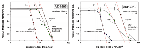
Based on the experimental results illustrated in figure 4, both AZ-1505 and ARP0-3510 would lose their contrast by a factor of 2, in addition to the dose requirement increase. As result, while it is possible to use both PRs for the hybrid process of both NIL and Optical (UV) lithography, the reduction in sensitivity and resolution are some of the compromises that need to be made.
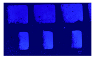
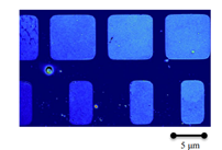
For the adhesive problem related to traditional PR, the AZ-1500 series resist was further evaluated by Dr. Jugessur in 2016. In short, to resolve the lift of pattern transfer resist during mold liftoff, the authors suggested the use of Teflon coating on the replica mold. Using a Teflon coating nanoimprint mold to reduce adhesion, the author was able to demonstrate the improvement in figure 5 illustrated [8].
Honeycomb Gratings
Giving the emergence of renewable energy in recent years, many researchers have published promising results involving the use of NIL to create grating nanostructures that improves the efficiency of thin-film solar cells. Two of the most widely adopted grating nanostructures to improve absorption of thin-film solar cells are based on honeycomb and periodic structures. Simply put, by increasing the order of diffraction and scattering, the path of the photons traveling through the solar cell (optical path length) is increased. As a result of the increased optical path length, it gives the thin silicon layer in a solar cell more chance to convert the photon into electrical current, therefore increase the short circuit current and the quantum efficiency of the solar cell [9].
It is also important to note that the abortion increase is mainly in the red part of the optical spectrum, as the blue and green light wavelength is still significantly higher than most thin-film solar cells with maximized absorption[9].
With that being said one of the most interesting uses of nanoimprint for solar cell is the utilization of roller-based NIL with UV curing. Using a roller-based system scaled to156 x 156 mm², the authors were able to demonstrate the feasibility of roller & UV-based NIL presented in figure xx [10]. Interestingly, the smaller contact area of the roller-based NIL could also reduce adhesion, and allows for a much smoother and controller demolding. Most importantly, with a smaller contact area through the roller-based NIP, the stamp pressure required is significantly reduced, which improves ‘homogeneity in terms of the residual layer thickness distribution across the substrates’ [10].
The stamp used in the experiment is based on PDMS, a much softer polymer in comparison. The pressure during the stamp is about 0.8 bar. While the authors did not specify exactly what pattern transfer resist was used, they did state that the pattern transfer resist is a negative tone resist with cross-linking, and UV curable with an efficiency of around to 100 mJ/cm2 depending on multiple variables, including actual wavelengths absorbed.
SWG
Nanostructure can be constructed using NIL to reduce reflection, and further improve the efficiency of solar applications. To start, antireflection grating, often referred to as subwavelength grating, works by reducing the number of diffraction orders. More specifically, when the size of the structure becomes subwavelength, it is possible to reduce the number of diffraction orders to 1. Therefore, in a perfect SWG with only the 0th order propagated, all higher order of diffraction become evanescent, which allows the SWG medium to become homogenous, and approximate with Snell’s law to some effective index(11).
SWG is a competing alternative to index-based anti-reflective coating. In addition, to achieve the miniature structure required for SWG, NIL is an attractive alternative to photolithography techniques with cost and throughput advantages.
Using the research work published by a group of researchers from ISE, the creation of NIL based SWG can be divided into 3 stages. To start, the substrate is first coated with porous sol-gel using dip-coating process, which is then tempered in an over at 500ºC for 10 min.
Secondly, the master structures for the SWG are created using holographic optical process based on argon ion laser. Next, based on the master structure created, a nickel replica is created as the actual stamp for the hot embossing process [11].
Lastly, the nickel stamp based on acrylate-modified polysiloxane is used to transfer the subwavelength grating structure onto glass. To reduce delamination, antiadhesive surfactant is used to pretreat the nickel master. The hot embossing takes place a pressure of around 4 MPa, with temperature higher than the glass transition temperature, which is followed by the curing stage UV irradiation. The author also discussed the possibility of transferring the stamp features onto the glass using roller-based process.
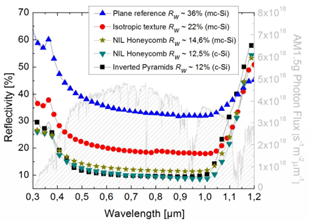
The difference in glass transmittance efficiency between Non-SWG and SWG based on NIL ranges from 8% to 4% improvement. The experiment was conducted on a 2mm thick glass pane at incidence of 8 degree. Due to the reduction in reflection, both ORMOCER and porous sol-gel based coating can achieved a much higher transmittance though the glass, especially at the shorter wavelength range [11].
SWG based on an alternative NIL process using soft embossing with spin coat is proposed by Yoshiaki Kanamori, Emmanuel Roy, and Yong Chen in 2004[13]. The soft nanoimprint stamp with spin coating technique does not require the additional temperature and pressure conditions, which simplifies the SWG creation through NIL.
Referred to as SNIL (Soft nanoimprint lithography), this alternative technique creates SWG under room temperature at low imprint pressure of less than <1 bar. Most importantly, the authors claim that soft flexible stamps enable a larger area imprint, due to the more conformable contact stamps make with silicon-mold. Finally yet importantly, since SNIL uses a soft stamp that is transparent, the author claims that it allows for a higher precision alignment during embossment [13].
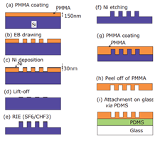
In summary, SNIL creates the SWG separately by spin coat PMMA coating onto a silicon stamp, which is then peeled off and attached to the glass via PDMS. Unlike hot embossing where the structure is stamped on top of the glass subtracted through a buffer layer, SNIL creates the PMMA based SWG on a separate silicon substrate, which is then attached to the glass using polydimethylsiloxane (PDMS) as the buffer layer.
There are multiple disadvantages to SNIL. To start, it requires an additional vaporized TMCS exposure stage to the silicon mold to facilitate the peel-off PMMA. It also requires degassing of PMMA after spin coat at room temperature, followed by heating treatment at 80 ºC for 30 min. Lastly, the author did not go into detail on how the PMMA is transferred onto the glass, or if the silicon mold created can be reused for a second or third time.
References
[1] Chou, S. Y. (1995). U.S. Patent No. 5,772,905. Washington, DC: U.S. Patent and Trademark Office.
[2] International Technology Roadmap for Semiconductors, 2003 Edition, “Lithography
[3] Cui, Zheng. “Nanofabrication: Principles, Capabilities and Limits”. Springer International Publishing, 2017. 234
[4]Cattoni, Andrea & Chen, Jing & Decanini, Dominique & Shi, Jian & Haghiri-Gosnet, Anne-Marie. (2011). Soft UV Nanoimprint Lithography: A Versatile Tool for Nanostructuration at the 20nm Scale. Recent Advances in Nanofabrication Techniques and Applications. . 10.5772/21874.
[5]K. Ansari, P.G. Shao, J.A. van Kan, A.A. Bettiol, F. Watt, Proton beam fabrication of nickel stamps for nanoimprint lithography, In Nuclear Instruments and Methods in Physics Research Section B: Beam Interactions with Materials and Atoms, Volume 231, Issues 1–4, 2005, Pages 407-412, ISSN 0168-583X, https://doi.org/10.1016/j.nimb.2005.01.091.
[6] Chien-Hung Lin, Rongshun Chen, “New approaches of mold fabrication for nanoimprint lithography,” Journal of Micro/Nanolithography, MEMS, and MOEMS 10(1), 011506 (1 January 2011). http://dx.doi.org.ezproxy.rit.edu/10.1117/1.3564881
[7] Khalid Dhima, Christian Steinberg, Saskia Möllenbeck, Andre Mayer, Hella-Christin Scheer, “Thermal nanoimprint (T-NIL) with photoresists for hybrid lithography”, Proc. SPIE 7985, 27th European Mask and Lithography Conference, 798506 (2 April 2011); doi: 10.1117/12.882805; http://dx.doi.org.ezproxy.rit.edu/10.1117/12.882805
[8]A. S. Jugessur, A. Zhang, Y. Lyu, “Nanoimprint of large-area optical gratings on a conventional photoresist using a teflon-coated nanoimprint mold”, Proc. SPIE 9759, Advanced Fabrication Technologies for Micro/Nano Optics and Photonics IX, 97591C (14 March 2016); doi: 10.1117/12.2211162; http://dx.doi.org/10.1117/12.2211162
[9]Dewan, R., & Knipp, D. (2009). Light trapping in thin-film silicon solar cells with integrated diffraction grating. Journal of Applied Physics, 106(7), 074901. doi:10.1063/1.3232236
[10] Benedikt Bläsi, Hubert Hauser, Christian Walk, Bernhard Michl, Aron Guttowski, Alexander Mellor, Jan Benick, Marius Peters, Sabrina Jüchter, Christine Wellens, Volker Kübler, Martin Hermle, Andreas J. Wolf, “Photon management structures for solar cells”, Proc. SPIE 8438, Photonics for Solar Energy Systems IV, 84380Q (2 May 2012); doi: 10.1117/12.921824; http://dx.doi.org.ezproxy.rit.edu/10.1117/12.921824
[11] H. Schmid, J & Cheben, Pavel & Janz, S & Lapointe, Jean & E, Post & A, Delâge & A, Densmore & B, Lamontagne & P, Waldron & Xu, DanXia. (2008). Subwavelength Grating Structures in Silicon-on-Insulator Waveguides. Advances in Optical Technologies. 2008. . 10.1155/2008/685489.
[12]A Gombert, W Glaubitt, K Rose, J Dreibholz, C Zanke, B Bläsi, A Heinzel, W Horbelt, D Sporn, W Döll, V Wittwer, J Luther, Glazing with very high solar transmittance, In Solar Energy, Volume 62, Issue 3, 1998, Pages 177-188, ISSN 0038-092X, https://doi.org/10.1016/S0038-092X(98)00008-5.
[13] Yoshiaki Kanamori, Emmanuel Roy, Yong Chen, “Fabrication of soft nanoimprint stamps and polymer subwavelength gratings by spin coating techniques”, Proc. SPIE 5635, Nanophotonics, Nanostructure, and Nanometrology, (9 February 2005); doi: 10.1117/12.571986; http://dx.doi.org.ezproxy.rit.edu/10.1117/12.571986
MACHINE VISION INTEGRATORS